This is the now classic symmetric IPS problem. The usual solution is nix the current mirrors. I think BC adds some resistors to load the current mirrors. I tried to create a common mode feedback but even with lots of ~servo filtering, it always created lots of 2nd order THD. Maybe that would be fine? But a single LTP can do better than 0.001% THD so I just wouldn't bother.

Your correct. However would this small fluctuation cause issues here for the cascodes that are operating as switches here. There an approach thats already popular with wolverine where it caters for the input signal also, would these be audible?2R+1C+1Zener would increase PSRR by 20X. Cost increase: 1 new resistor and 1 new capacitor per rail.
2R + 2Zener would increase PSRR by 100X. Cost increase: 1 new resistor and 1 new Zener per rail.
1R + 1 JFET + 2Zener would increase PSRR by 300X. Cost increase: 1 new resistor and 1 new JFET per rail.
"Works great" with 1R and 1Zener ... passes up some very cheap opportunities for much better performance.
Thanks,let me get on itSeen that in some of your other posts with parallel small dies or T0-92
Something I thought of trying as well.
sure many would overreact to it as well.
But was interesting to see.
Far as this design
common 3503/1381 could be used for Q4,Q16, Q11, Q13, Q17, Q18
Think it would really wake up the performance.
Be interesting to see the numbers in same sim
The output swings between that range -50 mV to +50 mV as expectedIf you already built a dozen or more of them, checked the bias currents of Q16 and Q4 for each of them and found that the spread is perfectly acceptable, then I agree. In that case, apparently the offset of the input stage and the current gain of the second stage is small enough for the conceptual issue I found not to be a big deal in practice.
If this design only exists as an LTSpice simulation, then I would advice you to put a DC voltage source in series with the base of one and only one of the four input transistors, do a DC sweep where this voltage source is swept from -50 mV to +50 mV and see what happens with the DC currents through Q16 and Q4. It's a simulation that can be run in a few minutes and it will give you an impression whether the issue I mentioned is a big deal or not.
They do track and the LTP gain is kept below 20dBI just now saw this thread. A mismatch in the differential pairs will cause Q4 and Q16 to have zero current or to burn out.
The differential pairs loaded by current mirrors have too much gain. A "feature" of the fully complementary amplifier is that the gain must be relatively low in order for the two halves to track.
Ed
The two control loops are antagonistic, think slewI agree with the guys expressing concerns. Was just thinking about it in a different way, which would be more along the lines of what might be its dynamical response be in the presence of noise? Say, for example, if one kicked one of the control loops to upset the output, then what would the dynamical response of the other control loop be, and how would the two loops settle (assuming the excited mode is sufficiently damped). Even if stable, what might the effect on sound be, depending on particular mismatches?
Pls share your implementationI was thinking of a fast common-mode loop, one that also ensures the signal currents through the two transistors are equal, rather than a slow one.
What happens with the currents through Q16 and Q4?The output swings between that range -50 mV to +50 mV as expected
Did you apply the offset to only one of the four input transistors? If you did, I don't understand why the output swings from -50 mV to +50 mV.
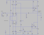
I thought of something like this, but it needs something extra to protect against destructive latch-up when QCM6 and QCM8 go in saturation.Pls share your implementation
Works great, we have to mimiclooks like normal emitter followers to me.
with emitter resistors and sharing same heatsink.
MJE340/350 is questionable choice.
as with any design everyone will nit pick it
We can minimize complexity by trusting the hfe behavior of the bjt usedI thought of something like this, but it needs something extra to protect against destructive latch-up when QCM6 and QCM8 go in saturation.
View attachment 1196017
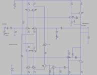
After remembering to include the plotwise directive, this seems to work well. The VAS current in both VAS transistors will necessarily be the same, save the OPS input current. So I just sense it on one side and inject a small servo current into the current mirrors (both) that sets the VAS current to a constant defined by the divider R11, R12.
Attachments
Marcel: " ... a fast common-mode loop, one that also ensures the signal currents through the two transistors are equal, rather than a slow one."
Pls share your implementation
An excellent opportunity to let Chat GPT exhibit its brilliant expertise at circuit design, don't you think? We all know Marcel is supremely talented; now give Chat GPT the chance to really shine.
The gain is proportional to the Hfe of Q4 and Q16. It is poorly controlled.They do track and the LTP gain is kept below 20dB
Leach's LTP has a tightly-controlled gain of ~2.
Ed
😉😆 thanks for your sense of humor, probably in the coming months she can do that, but why wait when we got usAn excellent opportunity to let Chat GPT exhibit its brilliant expertise at circuit design, don't you think? We all know Marcel is supremely talented; now give Chat GPT the chance to really shine.
- Home
- Amplifiers
- Solid State
- NOT Blameless Amplifier (Red)