Here's a challenge
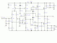
"Apart from that - the pole, introduced by the 100 pF capacitor and the FET's intrinsic capacitance might be much lower than intended - due to the high source impedance of the current mirror."
Ok Diogo, your mission is to calculate the frequency of the Miller pole in each design: with and without the current mirror. You'll learn a lot by trying to do this.
I sort of like the current mirror.
The new circuit looks ok but I'd be inclined to put a 50uF or so capacitor across the output bias adjustment pot so that the output bias doesn't get unduly modulated by the VAS current.
Why are you using a mosfet for the VAS and not a BJT?
Re: Here's a challenge
I wonder the same thing myself? I can't see any real benefits of a MOSFET here.
traderbam said:Why are you using a mosfet for the VAS and not a BJT?
I wonder the same thing myself? I can't see any real benefits of a MOSFET here.
I'm using a Mosfet for the VAS becouse I never did it before and I'm decided to make it work...........
OK, I can understand the reasons but be also beware of the rather high capacitancies you get just because of the MOSFET. I suggest that you bias this stage alone and test the gain and the frequency response. If it would be useful the gain must be 100-1000 at least and the bandwith with 1 kohm signal impedance (your collector resistor) 1-20 kHz.
This p-channel caps are there to ballance the output devices input capacitance since the hexfets IRF640 and IRF9640 aren't complementary.
This value is obtained in pratice and shows good performance, I did it using a square wave and comparing the the amplified signal, but i did it with the 1rst prototype, witchs have only one pair at the output.
This value is obtained in pratice and shows good performance, I did it using a square wave and comparing the the amplified signal, but i did it with the 1rst prototype, witchs have only one pair at the output.
Olá Diogo!!😉
You must use with the IRF mosfets a VBE with a transistor in contact with the eatsink...the IRF mosfets are vertical mosfets and have a positif temperature coeficient until they reach a current of several Amps.
The bias schema with a simple pot is only possible with the Hitachi's mosfets or equivalents!
Cumprimentos!!
Jorge Santos
Tube_Dude said:You must use with the IRF mosfets a VBE with a transistor in contact with the eatsink...the IRF mosfets are vertical mosfets and have a positif temperature coeficient until they reach a current of several Amps.
The bias schema with a simple pot is only possible with the Hitachi's mosfets or equivalents!
Yes, good point. Calculate for -10 mV / deg C as compensation.
In the original schematic you have shown 1k Ohm degen resistors in the current mirror. these are way too high, use between 100 and 220 Ohms. also the current in the first stage I would increase to 6 ma. Use about 470 Ohm resistor for this.
The biasing for the IRF devices is also in error. this won't produce enough forward bias. I would use a Vbe multiplier and mount it close to or on one of the o/p devices.
Anthony Holton
PS I have only had a quick glance at this schematic there maybe other errors.
🙂
The biasing for the IRF devices is also in error. this won't produce enough forward bias. I would use a Vbe multiplier and mount it close to or on one of the o/p devices.
Anthony Holton
PS I have only had a quick glance at this schematic there maybe other errors.
🙂
The design looks a lot like my lateral mosfet design.
Just use the values from that design.
http://www.aussieamplifiers.com/downloads/chepamp.pdf
Just use the values from that design.
http://www.aussieamplifiers.com/downloads/chepamp.pdf
- Status
- Not open for further replies.
- Home
- Amplifiers
- Solid State
- no working amplifier