
I guess the new font end are for those who already has Stasis amplifiers?
The thread is not for building Stasis amplifiers from "zero"?
One schematic shows an output stage with 2 x 15 parallel power transistors?
The thread is not for building Stasis amplifiers from "zero"?
One schematic shows an output stage with 2 x 15 parallel power transistors?
Thank you, thank you, THANK YOU! 
I wrote this a couple of years ago:
Stasis Traps
... so I will definitely build this, but I will have to make the layout fit the mounting-holes and the wiring of my S/150, so it can be a clean swap.
Drilling new holes in this classic is an absolute NO in my opinion! 😛
Guess it's time to try and figure out how to do circuit-board layout. 😱

Not too long ago I received a request for some help from an owner of
an old Threshold Stasis amp, whose amp was broken and where some
previous work had left some issues with the circuit board.
As many of you will know, I have lots of time on my hands 😉 and a
sentimental desire to revise old product in light of the wisdom I have
acquired in 50 years.
So.
I revised the circuit, making it more simple, and laying out a circuit board
which should be usable for all known versions with minor adaptation.
Attached are various schematics and graphics and also the gerber files
for the circuit board, which was made my pcbway.com, who will ask
what dimensions are, which is 5.5" x 3.5"
This thread will also serve as the location for asking additional questions
and so on.

I revised the circuit, making it more simple, and laying out a circuit board
which should be usable for all known versions with minor adaptation.
Stasis revival 😀 Thank you Mr. Pass

Many transistors are available in stock
https://www.mouser.fr/ProductDetail...ha2pyFadujkBBywZDMUAZwqtCoiCpEUnT%2BKJIUMYe4=
https://www.mouser.fr/datasheet/2/408/TTA004B_datasheet_en_20170109-1102732.pdf
the other Toshiba in near future back in stock december 2020 by thousand pcs.
TTC004B,Q Toshiba | Mouser
https://www.mouser.com/datasheet/2/408/TTC004B_datasheet_en_20180223-1102342.pdf
https://www.mouser.com/ProductDetai...hild/KSC2690AYSTU?qs=bfRUmXT2lZiU5sTvxbBu3A==
https://www.mouser.com/datasheet/2/308/KSC2690A-D-1810605.pdf
https://www.mouser.com/ProductDetai...2pyFadui%2BEXR26k20TBfWGjF%2BP0GyaHVFRcxYMvQ=
https://www.mouser.com/datasheet/2/308/KSA1220A-D-1810436.pdf
Cool news

Fantastic power TO-3 transistors are available in stock 
MJ21193G ON Semiconductor | Mouser
https://www.mouser.com/ProductDetai...=/ha2pyFadujEihMqaz/hhkq6TQqOjR1kS1vnU717vwU=
https://www.mouser.com/datasheet/2/308/MJ21193_D-1811377.pdf
MJ21193G ON Semiconductor | Mouser
https://www.mouser.com/ProductDetai...=/ha2pyFadujEihMqaz/hhkq6TQqOjR1kS1vnU717vwU=
https://www.mouser.com/datasheet/2/308/MJ21193_D-1811377.pdf
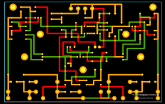
I see all top and bottom traces are doubled except cross traces and Q6, Q7 maybe for safety reasons if mask expose for some reason or damaged.
Mr. Pass what are benefits of doubling top and bottom traces?
Doubling trace thickness with just 1 oz copper?
P.S.: My OCD tells me there are missing top traces from +C to R23 and from C9 to V+ ... 😀
Mr. Pass what are benefits of doubling top and bottom traces?
Doubling trace thickness with just 1 oz copper?
P.S.: My OCD tells me there are missing top traces from +C to R23 and from C9 to V+ ... 😀
are they doubled??
Yes. Orange traces in the picture.
Mr Pass has built and tested it all OK so there are no traces missing on the pcb.
I think you did not understand what I meant..
Attachments
Last edited:
I still don't understand what you are trying to say - you need to be clearer.
On the picture from post #32 you can see traces from gerber file Nelson share.
Red color traces are top copper layer.
Green color traces are bottom copper layer.
Orange color are places where top and bottom copper layers match same route.
That means those fully orange traces are doubled from top and bottom.
Board obviously would would work without any doubled trace.
But there could be some interesting trick from Nelson I don't understand reason right now.
There are some logic.
Exception of traces that are double are the ones that cross both top and bottom layers, the ones that go to Q6, Q7 and the one I wrote "missing".
They could be doulbled too but they don't maybe for a reson maybe not.
May be trick have something to do with current go the path of least impedance or maybe it is overanalysis.. 🙄
I will also quote another trick from another thread as interesting and kind of relevant.
P.S.: Quite some while ago in this very thread, Nelson went to great pains to point out that if you put the + and - traces of a balanced signal on opposite sides of the board (or side-by-side) the two phases will be subject to the same magnetic/RF/whatever fields and thus the induced signal will cancel. I don't recall anyone "getting it." The boards I've seen certainly don't use the principle.
Happy Diyers thanks you very much Mr. Pass 
Toshiba back in stock today for revival XXI century Stasis amplifier version
https://www.mouser.com/ProductDetai...ha2pyFadujsCx4i9SwptWd73mY%2BPzNyyTI2b49gZww=
Toshiba back in stock today for revival XXI century Stasis amplifier version
https://www.mouser.com/ProductDetai...ha2pyFadujsCx4i9SwptWd73mY%2BPzNyyTI2b49gZww=

- Home
- Amplifiers
- Pass Labs
- New Stasis front end