Hey fellow DIYers,
recently I unplugged my good old GC modules in order to embedd 'em into speaker enclosures, thus making active speakers with GC amps. 😎
I thought I should take a look at their status regarding robustness, safety and connection quality - before dumping them into wooden enclosures.
It was then that I found out all of them (four channels total) oscillate when not connected to an input source. 😱
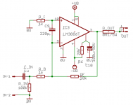
All of them are equal (see attachment), inverting topology with fairly low impedance level (1kOhm input, 18kOhm feedback).
I found out it does not matter wether I have:
- an input capacitor,
- a resistor between inverting input and ground,
- any combination of the above (i.e. resistor to ground before or after the input cap).
But it works with a real world input source - or a shorted input respectively.
This leads to the preliminary conclusion that a very low impedance current path from inverting input to ground is neccessary. But why? Non-inverting input is tied to ground with 1kOhm, inverting input (virtual ground point) sees 47kOhm when left open (100k in the attachment have been swapped along the way).
What's going on?
Thanks for any suggestions,
Sebastian.
PS: All channels are working fine when connected to any low impedance source, even after my analysis and parts swapping. 😉
recently I unplugged my good old GC modules in order to embedd 'em into speaker enclosures, thus making active speakers with GC amps. 😎
I thought I should take a look at their status regarding robustness, safety and connection quality - before dumping them into wooden enclosures.

It was then that I found out all of them (four channels total) oscillate when not connected to an input source. 😱
All of them are equal (see attachment), inverting topology with fairly low impedance level (1kOhm input, 18kOhm feedback).
I found out it does not matter wether I have:
- an input capacitor,
- a resistor between inverting input and ground,
- any combination of the above (i.e. resistor to ground before or after the input cap).
But it works with a real world input source - or a shorted input respectively.
This leads to the preliminary conclusion that a very low impedance current path from inverting input to ground is neccessary. But why? Non-inverting input is tied to ground with 1kOhm, inverting input (virtual ground point) sees 47kOhm when left open (100k in the attachment have been swapped along the way).
What's going on?
Thanks for any suggestions,
Sebastian.
PS: All channels are working fine when connected to any low impedance source, even after my analysis and parts swapping. 😉
Attachments
i think your pcb layout is good.
but you set the input impedance is too low.i prefer (22k input,470k feedback).
and i think the inverting gc must have an input dummy when the amp is ready to launch😎
z
but you set the input impedance is too low.i prefer (22k input,470k feedback).
and i think the inverting gc must have an input dummy when the amp is ready to launch😎
z
i think your pcb layout is good.
Thanks, that's good to hear. 😉
but you set the input impedance is too low.i prefer (22k input,470k feedback).
You actually find this low impedance setting a lot (in GC projects), even National recommend them in their BPA document AN-1192.
I choose it for the low noise level benefit.
and i think the inverting gc must have an input dummy when the amp is ready to launch😎
What do you mean by input dummy?
Cheers,
Sebastian.
Seba,
the answer is easy, yes, the input dummy.
When the input is open, the feedback divider (Rf/Rb) does not work, the circuit's noise gain (the gain when looking at in a noninverting view) is
1 + 18k/(1k+47k) = ~1.4
But you need at least a gain of 10 for the chip to be stable, better 15 or more. Now, your gain also depends on the source's (or pot's) output impedance, if it is more than about 1k you might get in trouble. So if you were to lower R_IN to 1k it would be right on the edge of stability with open input, and you would need a largish input cap and a source that can drive 500Ohms instead of 1k (ah, do the math for the input cap, it is way to small, it gets loaded with 1k or less, as shown. You need something like 47uF or so).
Also, the 220pF can be a problem source, although it is shown in the datasheet it still not a good thing to do, if one follows loop stability theory. Which says for this chip: at high frequencies you need a noise gain (the noninverting gain) of 10 or more.
The 1k an the +IN doesn't matter much, it controlles offset a little but has nothing to do with gain.
That's why normally a buffer is preferred for the inverting config, it's all about controlled conditions ;-)
Ah, R_out (0.1R) is of no worth, unless you put it in to have a controlled output impedance of just that value (but which gets swamped as soon as you use connectors and cables).
- Klaus (greetings from P'Berg, btw)
Hi Klaus,
m'kay, I'll take some time to get this sorted.
Damn, I wish it was difficult! 😀
This is actually the answer I was overlooking, spot on!
I had thought about RF, grounding scheme, etc.
But I had forgotten that the LM38x6 is not unity gain stable!
I'm aware of that 1uF and 1kOhm forms a way to high pole (or has a way too small time constant). The values you see are the result of trial and error to find a relation between component choice and oscillation frequency.
BTW, the speaker it powers is a mid/high unit, so no bass is required (but that's not why I chose 1uF, it was just the last update I made to the schematic during testing).
I think it's useful, although too large considering the impedance level. That's probably what you meant.
Who's claiming any different? 😉
It's there to minimize offset, and that's exactly what it does. 900 something Ohm would be better according to my calculation, but 1kOhm suffices to keep offset voltage up to spec (a couple of millivolts).
I thought about leaving it out in the process of troubleshooting, but certainly don't feel the need any more. 🙂
Don't laugh, they were intended to get an input buffer. They had originally been designed to become equipped with their respective active crossover filter.
And as they will get their buffer inside the speaker enclosures I plan on putting them in, I'd say all is well! 😀
It's of considerable worth: current limiting in case of an output short. 🙂
Nationals protection circuitry is good, but as I wanted the modules to be versatile, I thought: why not play safe. 😉
---
Sooo, I'd say my best bet is to raise the impedance level by a factor of 10 (using 10kOhm and 220kOhm) and see what happens, right? Could be the solution to the instability, the input filtering and the decoupling problem. I'd say a slightly increased noise floor into the tweeter's voice coil is better than a 30V triangle wave. 😱
Sebastian (greetings from L'Berg, btw)
m'kay, I'll take some time to get this sorted.
the answer is easy, yes, the input dummy.
Damn, I wish it was difficult! 😀
When the input is open, the feedback divider (Rf/Rb) does not work [...] but you need at least a gain of 10 for the chip to be stable
This is actually the answer I was overlooking, spot on!

I had thought about RF, grounding scheme, etc.
But I had forgotten that the LM38x6 is not unity gain stable!

(ah, do the math for the input cap, it is way to small, it gets loaded with 1k or less, as shown. You need something like 47uF or so).
I'm aware of that 1uF and 1kOhm forms a way to high pole (or has a way too small time constant). The values you see are the result of trial and error to find a relation between component choice and oscillation frequency.
BTW, the speaker it powers is a mid/high unit, so no bass is required (but that's not why I chose 1uF, it was just the last update I made to the schematic during testing).
Also, the 220pF can be a problem source, although it is shown in the datasheet it still not a good thing to do, if one follows loop stability theory. Which says for this chip: at high frequencies you need a noise gain (the noninverting gain) of 10 or more.
I think it's useful, although too large considering the impedance level. That's probably what you meant.
The 1k an the +IN doesn't matter much, it controlles offset a little but has nothing to do with gain.
Who's claiming any different? 😉
It's there to minimize offset, and that's exactly what it does. 900 something Ohm would be better according to my calculation, but 1kOhm suffices to keep offset voltage up to spec (a couple of millivolts).
I thought about leaving it out in the process of troubleshooting, but certainly don't feel the need any more. 🙂
That's why normally a buffer is preferred for the inverting config, it's all about controlled conditions ;-)
Don't laugh, they were intended to get an input buffer. They had originally been designed to become equipped with their respective active crossover filter.
And as they will get their buffer inside the speaker enclosures I plan on putting them in, I'd say all is well! 😀
Ah, R_out (0.1R) is of no worth, unless you put it in to have a controlled output impedance of just that value (but which gets swamped as soon as you use connectors and cables).
It's of considerable worth: current limiting in case of an output short. 🙂
Nationals protection circuitry is good, but as I wanted the modules to be versatile, I thought: why not play safe. 😉
---
Sooo, I'd say my best bet is to raise the impedance level by a factor of 10 (using 10kOhm and 220kOhm) and see what happens, right? Could be the solution to the instability, the input filtering and the decoupling problem. I'd say a slightly increased noise floor into the tweeter's voice coil is better than a 30V triangle wave. 😱
Sebastian (greetings from L'Berg, btw)
three options:
1.) fit an input buffer
2.) convert to non-inverting
3.) try fiddling with the impedances to cobble together a badly implemented inverting amplifier.
1.) fit an input buffer
2.) convert to non-inverting
3.) try fiddling with the impedances to cobble together a badly implemented inverting amplifier.
Hi Andrew,
let's see... 🙂
Will be done in the future, but for the moment the modules shall be safe and easy to use (i.e. harmless if the wife pulls a plug).
Not possible with the current PCB. I will design a non-inverting amp the next time. 😉
Now I'm interested why you say that. I see inverting GC implementations a lot in these forums and on the net. 1k/21k with buffer or 20k/220k without buffer are very common and tried approaches.
What change to the existing topology (and PCB) would you recommend in order to prevent bad quality and/or instability?
Sebastian.
let's see... 🙂
fit an input buffer
Will be done in the future, but for the moment the modules shall be safe and easy to use (i.e. harmless if the wife pulls a plug).
convert to non-inverting
Not possible with the current PCB. I will design a non-inverting amp the next time. 😉
try fiddling with the impedances to cobble together a badly implemented inverting amplifier.
Now I'm interested why you say that. I see inverting GC implementations a lot in these forums and on the net. 1k/21k with buffer or 20k/220k without buffer are very common and tried approaches.
What change to the existing topology (and PCB) would you recommend in order to prevent bad quality and/or instability?
Sebastian.
I've found the time to investigate a little further.
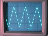
The attached shot shows the oscillation of the low impedance version (1kOhm/18kOhm).
This is measured at the after R_out with open (floating) input.
With the input shorted, the output is almost dead silent.
The attached shot shows the oscillation of the low impedance version (1kOhm/18kOhm).
This is measured at the after R_out with open (floating) input.
With the input shorted, the output is almost dead silent.
Attachments
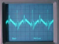
This next shot shows the high impedance version (10kOhm/220kOhm).
This is with the input shorted to ground, so it's the best I can get with this configuration!
I don't get it. What makes this high impedance version swing, especially at such a high frequency?
Any help is appreciated.
Sebastian.
This is with the input shorted to ground, so it's the best I can get with this configuration!
I don't get it. What makes this high impedance version swing, especially at such a high frequency?
Any help is appreciated.

Sebastian.
Attachments
Looks like with the high impedance level, you lowered the frequency of a parasitic pole (node impdance + input/stray capacitance at the inverting input). And now, if still present in your circuit, the 220pF is probably major part of the problem, adding deliberately to this capacitance (that's why I said it is dangerous), the zero introduced by the 1k is way to high, thus the 220pF can be seen as going more or less "directly" to GND.
Also, you might have now significant parasitic coupling from the output/supply to the input(s) and more nasty stuff of sorts... all due to the too high impedance level.
For a thorough discussion on these matters, see
http://eportal.apexmicrotech.com/mainsite/pdf/an19u.pdf
and
http://www.ti.com/litv/pdf/sboa015
Some lower supply voltage is easily derived from the rails, then you could add a buffer, built ie on a strip of veroboard, and you get rid of all the problems, turning down the impedances to the lower levels again...
- Klaus
Klaus,
thanks for your reply, very nice to have someone knowledgable looking at it. 😉
In order to check this possibility, I'll take another look at my grounding scheme.
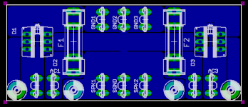
At the moment, my supply has a power ground star and a signal ground star. Both are sitting close to each other on the PSU board and meet via a short and thick copper trace.
The power ground is split, sinking (and sourcing) current for the positive supply capacitor and it's negative supply counter part via separate links.
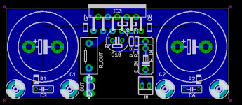
So the above PCB has three connections to the PSU star: From the "left" supply capacitor, the "right" supply capacitor, and the signal input (see attachment below).
I thought this would reduce hum and buzz by providing separate current return paths of low impedance for every part of the circuit.
But while this seems to work properly (no hum or noise audible), maybe this has introduced some stray capacitance or inductance I didn't think of! According to the high frequency and low amplitude of the oscillation, we're talking about Nanohenrys and Picofarads.
Does anyone have any idea about my grounding scheme's possible inadequacies?
The 220pF capacitor went out of the circuit as my first measure.
There's also no 1kOhm resistor in the circuit any more.
The part denominated as R_in has been tried down low to a short (0 Ohms), the problem persists no matter if I shift R_in in front of C_in.
Thanks for the links, I'll give both documents a read as soon as I can.
I am familiar with bode plot discussion, the influence of poles and zeroes on transfer functions, basic filter theory and signal processing in general, etc.
I just didn't expect so many difficulties with a tried and proven circuit.
As said above, this will happen in the future. I just can't accept that the circuit shouldn't work without it. I still expect an analytical (or maybe lucky) solution to be easier, quicker and cheaper than four improvised buffers (that would have to be thrown out again later anyway).
Thanks for any help again 🙂
Sebastian.
thanks for your reply, very nice to have someone knowledgable looking at it. 😉
Looks like with the high impedance level, you lowered the frequency of a parasitic pole (node impdance + input/stray capacitance at the inverting input).
In order to check this possibility, I'll take another look at my grounding scheme.
At the moment, my supply has a power ground star and a signal ground star. Both are sitting close to each other on the PSU board and meet via a short and thick copper trace.
The power ground is split, sinking (and sourcing) current for the positive supply capacitor and it's negative supply counter part via separate links.
So the above PCB has three connections to the PSU star: From the "left" supply capacitor, the "right" supply capacitor, and the signal input (see attachment below).
I thought this would reduce hum and buzz by providing separate current return paths of low impedance for every part of the circuit.
But while this seems to work properly (no hum or noise audible), maybe this has introduced some stray capacitance or inductance I didn't think of! According to the high frequency and low amplitude of the oscillation, we're talking about Nanohenrys and Picofarads.
Does anyone have any idea about my grounding scheme's possible inadequacies?
the 220pF is probably major part of the problem
The 220pF capacitor went out of the circuit as my first measure.
the zero introduced by the 1k is way to high
There's also no 1kOhm resistor in the circuit any more.
The part denominated as R_in has been tried down low to a short (0 Ohms), the problem persists no matter if I shift R_in in front of C_in.
For a thorough discussion on these matters, see http://eportal.apexmicrotech.com/mainsite/pdf/an19u.pdf and http://www.ti.com/litv/pdf/sboa015
Thanks for the links, I'll give both documents a read as soon as I can.
I am familiar with bode plot discussion, the influence of poles and zeroes on transfer functions, basic filter theory and signal processing in general, etc.
I just didn't expect so many difficulties with a tried and proven circuit.

you could add a buffer
As said above, this will happen in the future. I just can't accept that the circuit shouldn't work without it. I still expect an analytical (or maybe lucky) solution to be easier, quicker and cheaper than four improvised buffers (that would have to be thrown out again later anyway).
Thanks for any help again 🙂
Sebastian.
Attachments
i don't understand your power supply.
have you use CT transformer?I wonder if the psu in working order?have you checked the terminal voltage?
i appreciate your patience🙂 i think the igc should work without buffer.
p.s.
do you have a photo of your amp?
zang
have you use CT transformer?I wonder if the psu in working order?have you checked the terminal voltage?
I just can't accept that the circuit shouldn't work without it. I still expect an analytical (or maybe lucky) solution to be easier, quicker and cheaper than four improvised buffers (that would have to be thrown out again later anyway).
i appreciate your patience🙂 i think the igc should work without buffer.
p.s.
do you have a photo of your amp?
zang
Seba,
I think your PSU layout is just fine (from what one can tell without fotos)...
... but this has nothing to do with the stray capacitance I mentioned.
Analytical solution?... go non-inverting, which requires nothing more that to rip up and patch you amp-PCBs a little, not a problem IMHO. You even have a lot of space left in the center area of the pcb, drill a few holes and stuff the parts you need there, rewire the new input to the pinheader etc. At least that's what I would do (you won't believe how much this type of "PCB revisioning" is used in the industry -- "new PCB? Naw! Let's hire some students who will happily modify this batch of, er, 2000 boards here. Nobody will see it anyway").
- Klaus
- Status
- Not open for further replies.
- Home
- Amplifiers
- Chip Amps
- New problems with old Gainclone...
