r_jik45 said:Hi Digi01,
Nice work, thank you for sharing it.
I suppose I missed something... but why are D1 and D2 (from the original schematic) not here anymore?
Have a nice day...
Yes,I have removed them.
best
Zang
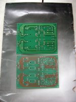
Hi Zang,
The boards look good.
One question: What is the recommended way of
mounting the mosfets? Do we just mount them
flat on the PCB with small heatsinks?
Thanks,
Dennis
The boards look good.
One question: What is the recommended way of
mounting the mosfets? Do we just mount them
flat on the PCB with small heatsinks?
Thanks,
Dennis
Hi Zang ,
the boards arrived today ,
nice work !
Thanx again for this Group Buy
Greetings from Germany
Jürgen
the boards arrived today ,
nice work !
Thanx again for this Group Buy
Greetings from Germany
Jürgen
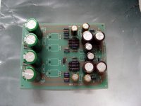
thanks all.
Partlist below:
R1,R2,R3,R8=1K
R4=20K
R5,R6=220
R7=33K
R9=220K*
R13=100K*
R14=180K*
R15=470
R10,R11,R12=2.2,1W
R18=5.6,3W
C1,C3=100uf/35V
C2=4.7u/100v
C4,C5=1000uf/50v
C6,C7=2200uf/50v
D1,D2,D3,D4=1N4007
Yes,you can mount them flat on the top of pcb with small heatsink or mount them on the chassis.
Cabdriver said:the board looks great! Do you have a parts list already?
thanx!
Partlist below:
R1,R2,R3,R8=1K
R4=20K
R5,R6=220
R7=33K
R9=220K*
R13=100K*
R14=180K*
R15=470
R10,R11,R12=2.2,1W
R18=5.6,3W
C1,C3=100uf/35V
C2=4.7u/100v
C4,C5=1000uf/50v
C6,C7=2200uf/50v
D1,D2,D3,D4=1N4007
Dennis Hui said:Hi Zang,
The boards look good.
One question: What is the recommended way of
mounting the mosfets? Do we just mount them
flat on the PCB with small heatsinks?
Thanks,
Dennis
Yes,you can mount them flat on the top of pcb with small heatsink or mount them on the chassis.
Hi Zang,
I received my boards yesterday. Thanks for your fast delivery, the nice PCBs, and the excellent parts.
Regards,
Zoltan
I received my boards yesterday. Thanks for your fast delivery, the nice PCBs, and the excellent parts.
Regards,
Zoltan
just received the boards here as well!
so whos going to be the first to have this amp finished? 😉
grtz
so whos going to be the first to have this amp finished? 😉
grtz
Got boards today!
Zang, is it true your girlfriend agreed to marry you? Is she crazy? She know what she's getting into by marrying and Engineer? I am joking..
CONGRATULATIONS!!

Zang, is it true your girlfriend agreed to marry you? Is she crazy? She know what she's getting into by marrying and Engineer? I am joking..
CONGRATULATIONS!!
Hi Zang,
did you receive my last PMs?
I read somewhere your personal mail doesn't work correctly and I haven't received any answer for some weeks about my last e_mails.
I'm asking for informations about my (already paid) booking for 1 MiniZen board and 2 SOHA PCBs. Are you sending them or are there some problems?
Thanks
Nicola
Hi Zang,
I too have not received my (2) PCBs. Do you
remember when they were mailed?
Thanks,
Dennis
I too have not received my (2) PCBs. Do you
remember when they were mailed?
Thanks,
Dennis
Hi Zang.
I also just wanted to make sure you remember me. Though I am in no hurry to get them so just take your time.
Thanks
Martin
I also just wanted to make sure you remember me. Though I am in no hurry to get them so just take your time.
Thanks
Martin
Zang,
I'm still awaiting my boards. I pinged you via e-mail, but haven't seen a response back from you yet. Can you provide any updates on my order?
Thanks,
Mike
I'm still awaiting my boards. I pinged you via e-mail, but haven't seen a response back from you yet. Can you provide any updates on my order?
Thanks,
Mike
Q3 position?
Hi,
I'm making this amplier too and while soldering the parts I wanted to be sure regarding how to put Q3 (ZTX450/2N2222); for that I checked on Digi01's board in a previous post (LINK).
According to the attached file and to the transistor datasheet, the pin are E, B, C from top (Q1 side) to bottom (C4 side), but according to the schematic it should be B, C, E (B connected to R3, C3, bias / C connected to R2, R5 / E connected to C1, R10,9,11, etc)
So here is my question: don't you have problems when you connect Q3 the way it is presented on the drawing? Don't you have to rotate it in order to connect it according to the schematic? 😕
Thanks in advance for your reply,
And have a nice end of weekend.
- Home
- Group Buys
- New MINI ZEN Headphone Amp PCB group order...