I wanted to share a new line stage idea that developed out of some work I was doing with the Zen IV converter. I posted it here instead of in the analog line forum as it is more in line with this one. I looked for a Balanced to SE conversion stage that was as simple, elegant, and performed as closely to the Zen IV as possible. No ICs for this one obviously, and every discrete opamp I modeled that performed well became too complex to satisfy the “simple and elegant” requirements.
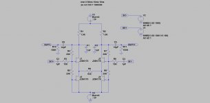
Here is what I came up with - It is similar to an Aleph P, only built with JFETs. Unlike simple followers, it can support gains reasonably up to 10 or possibly higher, can support voltages of +/-10 to +/-20V or higher, and can operate of a single supply of between 10 and 40V or so.
If you have a problem with capacitors in the signal path, you probably should look away… Just kidding, no more than usual for something this simple!
J2 and J4 are current sinks for J1 and J3. The gain is defined as the parallel combination of R4 and R5 divided by R3. R6, R7, and R8 serve the same purpose for the other side. Gain Resistor R9 is feedback between the sides and is sized to set the gain accurately. The rest of the circuit is pretty much self explanatory. The HF rolloff caps C1 and C2 are optional based on your taste. The input and output are necessary to prevent offset concerns with other equipment.
I tried changing resistors R1 and R2 to into current sources, but the circuit suffered for it. The gain of these devices is jut to low from what I can figure. Likewise, reducing the current in J2 and J4 with source resistors also degraded the performance.
The circuit as drawn starts to clip at about 5.5Vrms, or 15V p-p. Should be enough for most needs. Distortion from the models looks to be below 0.005% at 1Vrms output. It rises as you add gain, but still looks to be below .01% at a gain of 10...
To increase the gain, first decrease R3 and R6 and R9. R3 and R6 are set at 10K for unity gain to keep the input current low (and the input caps small!) G=5 is set by R3, R6 = 1K; R4, R5, R7, R8 = 20K, and R9 as 320 ohm. To set the G=10 R3, R6 = 1K; R4, R5, R7, R8 = 40K, and R9 as 160 ohm.
Back to where I started, if you connect your SE amp to the positive output and ground, all appearance are that it will work as a nice balanced to SE converter. if you need to invert 180 degrees for some reason. It is there for you in the negative output.
I welcome any comments and feedback. The circuit is fairly well optimized, although I may have missed something. I may not get back quickly, so please be understanding if I do not reply promptly. I also hope that someone with both SE and balanced input amplifiers will test this somewhere along the way to see if it compares well for that purpose.

Dave
Here is what I came up with - It is similar to an Aleph P, only built with JFETs. Unlike simple followers, it can support gains reasonably up to 10 or possibly higher, can support voltages of +/-10 to +/-20V or higher, and can operate of a single supply of between 10 and 40V or so.
If you have a problem with capacitors in the signal path, you probably should look away… Just kidding, no more than usual for something this simple!
J2 and J4 are current sinks for J1 and J3. The gain is defined as the parallel combination of R4 and R5 divided by R3. R6, R7, and R8 serve the same purpose for the other side. Gain Resistor R9 is feedback between the sides and is sized to set the gain accurately. The rest of the circuit is pretty much self explanatory. The HF rolloff caps C1 and C2 are optional based on your taste. The input and output are necessary to prevent offset concerns with other equipment.
I tried changing resistors R1 and R2 to into current sources, but the circuit suffered for it. The gain of these devices is jut to low from what I can figure. Likewise, reducing the current in J2 and J4 with source resistors also degraded the performance.
The circuit as drawn starts to clip at about 5.5Vrms, or 15V p-p. Should be enough for most needs. Distortion from the models looks to be below 0.005% at 1Vrms output. It rises as you add gain, but still looks to be below .01% at a gain of 10...
To increase the gain, first decrease R3 and R6 and R9. R3 and R6 are set at 10K for unity gain to keep the input current low (and the input caps small!) G=5 is set by R3, R6 = 1K; R4, R5, R7, R8 = 20K, and R9 as 320 ohm. To set the G=10 R3, R6 = 1K; R4, R5, R7, R8 = 40K, and R9 as 160 ohm.
Back to where I started, if you connect your SE amp to the positive output and ground, all appearance are that it will work as a nice balanced to SE converter. if you need to invert 180 degrees for some reason. It is there for you in the negative output.
I welcome any comments and feedback. The circuit is fairly well optimized, although I may have missed something. I may not get back quickly, so please be understanding if I do not reply promptly. I also hope that someone with both SE and balanced input amplifiers will test this somewhere along the way to see if it compares well for that purpose.
Dave
Attachments
we made something like this previously ;
dunno how's named - maybe Jfet BOSOZ or something like that
full SUSY , DC coupled inputs etc
in any case - you made nice work
dunno how's named - maybe Jfet BOSOZ or something like that
full SUSY , DC coupled inputs etc
in any case - you made nice work
we made something like this previously ;
dunno how's named - maybe Jfet BOSOZ or something like that
full SUSY , DC coupled inputs etc
in any case - you made nice work
Hi Zen Mod,
Thanks for the compliment!
Also thanks for the original project name. A search led me right to it... Some of those discouraging sim results look very familiar. I never could get the CCS replacements for the resistors to work well enough either... It can work but the distortion goes up considerably. Never got to a cascode, need to try it.
I will also go back and look at the input caps to see if they are really necessary. I started with fairly low gain resistors at the input. With the final values, input caps might not be necessary at all. Need to check at different gains and input levels as well.
Maybe there will be some interest in a JFET version again.
Dave
Thanks nAr.
I also wanted to point out for everyone that the gain for SE output is 1/2 that of Balanced output. The gain figures in the original post are for balanced out. The clipping number for the output is per side, so for balanced it would be twice as much. I just want to make sure there is no confusion...
Enjoy!
Dave
A few more details for those interested -
On the input capacitor question, removing the caps causes a modest rise in distortion. Offset current at the input I believe. I suggest you could take them out or leave them there, depending on what you think when you listen to it.
As drawn the circuit bandwidth is limited by the input capacitor. At unity gain, the -3db point is ~10Hz. when increasing the gain to 5, it is at ~20Hz. Increasing the input cap to 2uF keeps the -3db point the same, ~10Hz. The output caps can be reduced to 2uF as well with a 10K load on the output with about the same -3db point. If you want to drive into 600 ohms differential, leave them large...
Patirck,
Very nice information there. This appears in line with the changes you made to the F5 and F5X diff pair to more closely match the parts. Reading through it also is eye opening when it comes to the performance of a discrete opamp-like implementation with a conventional jfet diff pair and current source. Without more gain (more stages), current sources, degeneration, cascodes, etc, I would not have gotten where I wanted to be... It answered just about all of the questions I had! Thank you.
Interesting reading in the Blowtorch threads as well. I did not make it far enough to see if anyone made a PCB for DIY use. I like the JC80 circuit, it reminds me of a certain xamp in the works...
Dave
I was trying to point out to you the difference between single ended and complementary diff pair.
Patrick
Patrick
Hi Patrick,
Thank you. I will be doing some complimentary work in the future I believe! It was enlightening for SE pair performance as well...
Dave
Thank you. I will be doing some complimentary work in the future I believe! It was enlightening for SE pair performance as well...
Dave
Dave, this looks elegantly simple, kudos! I'm really surprised there hasn't been much interest.
I just ordered a pile of 170s to mess with and try it both SE and balanced and compare it to the P.
I was thinking about using voltage referenced current sinks instead of the 170s. I don't do any sims, just my ears.
I just ordered a pile of 170s to mess with and try it both SE and balanced and compare it to the P.
I was thinking about using voltage referenced current sinks instead of the 170s. I don't do any sims, just my ears.
Hi Bill,
Thank you. Yes, although it took quite a few back loops to figure out how to make it work. The great thing was that it fit well over the devices I had already chosen for the output follower for the balanced the Zen I/V board. The addition of a handful of resistors allowed me to add it in without much efort.
I am interested in impressions and comparisions to other circuits if you or anyone else has the time to do so. I will be testing as balanced to SE stage as I do not yet have a fully balanced amplifier... Should be rectifing that soon!
Thanks,
Dave
Last edited:
Hi Bill,
The models were idss of 12mA. I plan to use BL grade, 8-12 mA. All four FETs should be matched if possible. Match the top and bottom FET to each other at a minimum and keep the two sides as equal as possible to minimize the differential offset. Since each side has a seperate CCS, the supply current is roughly 2x idss plus the modulation current across the 1.5K resistors, something around 1mA at 1Vrms out per side. The input current is in the hundreds of microamps range per side, depending on the feedback resistance.
Dave
Last edited:
I am new and limited in my understanding so i have some questions if you don't mind. Is the gate of J2/J4 biased by the current passing thought the fet. If so, what determines this current
I am new and limited in my understanding so i have some questions if you don't mind. Is the gate of J2/J4 biased by the current passing thought the fet. If so, what determines this current
J2 and J4 are two independant current sources. They conveniently run at IDSS and serve the purpose to bias the diff. pair J1 / J3 whose swing develops at the resitor drains 1K5. R4 and R7 are feedback resistors. One can control the gain varying R9
So J2/4 sinks roughly 12mA of current because the Vgs of J2/4 rest at 0v. What voltage does the gate of J1/3 see when the power is on and there is no input? 10V. If so, when a signal is introduced, there is a change to Vds of J1/3 and R4/R7 see this voltage and feed it back to the gate of J1/3. Is all this happening on both sides or is this one side at a time depending on the polarity of the incoming signal?
Last edited:
So J2/4 sinks roughly 12mA of current because the Vgs of J2/4 rest at 0v. What voltage does the gate of J1/3 see when the power is on and there is no input? 10V. If so, when a signal is introduced, there is a change to Vds of J1/3 and R4/R7 see this voltage and feed it back to the gate of J1/3. Is all this happening on both sides or is this one side at a time depending on the polarity of the incoming signal?
I'm unsure Vgs of J2/J4 stays at 0 volt DC. This is why we see the use of coupling caps I guess. The 2 currents sinks are roughly at IDSS i.e. saturation. If the drains of the diff pair run roughly at 10V, then R4/R5 from there to negative rail -20V act at DC as a voltage divider, so gates of the diff pair should be at -5V or so.
I guess feedback occurs strictly at the same time on the 2 sides, as when one out is +, the other out is - for sure ( phase inverted )
Perhaps current sinks are difficult to implement on the positive side, because of the low Gm of the devices and also they should strictly be equal to the downward current sinks, to let flow strictly equal currents. Perhaps another idea (to get all the juice of the jfet pair) would be to keep the actual current sinks on V- and implement a cascode on the V+ side. Maybe you'll need to raise the V+ in order for it to work properly, and define more precise currents than actual IDSS of devices that varies even if small bits. So yes, a source resistor 🙂fitzfish said:I tried changing resistors R1 and R2 to into current sources, but the circuit suffered for it. The gain of these devices is jut to low from what I can figure.
I guess you talk about adding a resistor between sources of J2/J4 and negative rail, on the 2 sides. Maybe degrading has to do with the actual gate polarization. Or, added resistor= likely always lower current i.e. degraded measured performance.fitzfish said:Likewise, reducing the current in J2 and J4 with source resistors also degraded the performance.
You could also completely leave out R9 as it rolls off gain, and have different feedback resistor values in order to control gain completely from here 🙂
I'm still working on an excellent circuit made by Uli couple of years ago. See some very interesting points in it 🙂 🙂 🙂 I'm attaching schematic of it here, and also link to the old thread.
http://www.diyaudio.com/forums/pass-labs/12747-x-modul.html
Regards,
nAr
Attachments

- Status
- Not open for further replies.
- Home
- Amplifiers
- Pass Labs
- New Line Stage