It is so saddening to see how LJM customers persist exibiting absolute lack of self-respect and LJMs' utter disrespect for his customers. This travesty is mutual. Perhaps this is what drives people to buying a fake Rollex - a false feeling of posessing something of value.

I do wish you'd keep your arrogant opinions to yourself. No one is interested.
You have criticised LJM and now are disparaging members who have bought one of his products.
Go and make a nuisance of yourself on another thread if you don't like LJM's products.
You have criticised LJM and now are disparaging members who have bought one of his products.
Go and make a nuisance of yourself on another thread if you don't like LJM's products.
I'm sorry, it isn't just my arrogant opinion but the Truth is UGLY:keep your arrogant opinions to yourself. No one is interested.
Hi,
the two reverse engineered schematics (Youtube, resp. #18) show a difference in the emitter-connections of the drivers.
In Mr. Beeny´s Youtube schematic the drivers are connected to the output instead of the output transistor´s collectors and collector resistors.
The output stage probabely ceases functioning as a CFP or Sziklai.
Maybe just an error in the process of reverse engineering??
I rather think, that the schematic in #18 is the correct one.
Still though it looks to me as if the L12-5 is a try to reduce parts number count and cost even more compared to the L12-2s to L12-4s.
Seemingly the biasing of the input stage current source went wrong, the base-stopper resistors are missing and the exclusion of the C4793 VAS transistor from a common thermal link to the bias generator could generate problems ... besides a seemingly far form optimal PCB layout.
As more facts and flaws are turning up, I wouldn´t recommend the LJM 12-5 amps.
I think I will assing a warning note on my website, since quite a number of threads, Youtube vids and websites copied and/or related to my reengineered schematics of the L12-2 ... which I think is still a really decent and cost-efficient design.
jauu
Calvin
Have we fallen so low to accept what the little crook did instead of asking a question:
Are we ready to let him do this?
Look: we are entitled to have technical data of the product. Instead, there is a product designed to deceive us. He has introduced extra fake leads into the board to prevent understanding the circuit. Also, he obfuscated the design by introducing the »FET« component which is a double SMD BJT masked with glue. He also has stripped the design to the bare functional minimum by omitting regular design components. By doing this he made layout prone to oscillation. And he doesn't care. I am 100% sure he will continue selling this garbage. He did the same with L20SE - I told him that his product is an oscillator, but he doesn't care.
So, I am asking you another simple question:
Are we really ready to accept this insult?
Board finished and installed side by side with l12-2 Ver 4, for fun I connect left channel to Ver 4 and right channel to Ver 5, the gain is the same so no difference in sound level, it is soon to compare que quality.
What i suspect to be the reason for the oscilation turned out to be confirmed, I changed the circuit (attached is the schematic with the simple change), the 33uF is now bettween two 10K resistors and it is very stable.
I test it with a 4 ohm resistor but I did not push it to max yet,
Tomorrow I will come with new information. Thanks
Attachments

I forgot to mention that the testing probe of the oscilisope was switched to 10X, so 2.17V rms are in reality 21,7. The offset at the output is 0,8 mv (very good compared to the L12-2 Ver 4 board with 3 mV), and the bias is adjusted to 3 mv, The drivers are the only components to get hot, as Michael Benny mention they work at around 40 ºC.
Hi,
I´d like to repeat the Q from #24, where I asked if someone could clarify the actual output stage schematic .... wether it may be Mr. Beeny´s sketch,
or Vit4min4s´s schematic in #26?
Also I´d like to know if the output transistors are the 1186/2837 standardly mounted or the 03202G/0281G?
jauu
Calvin
Good morning Calvin, the kit I received comes with Onsemi 03202G/0281G. I am curious how it works with the Sanken ones, because I have two L12-2 ver4 kits with 1186/2837 that are not assembled yet I will test them on this new board and let you know.
I am almost sure that the circuit that I post is correct, the voltage drop measured in the 0.1 ohm resistor needs to include the drivers current.
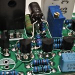
I leave a photo of the change I made to the board, it does not look preety but for testing is fine. 🤣
I am almost sure that the circuit that I post is correct, the voltage drop measured in the 0.1 ohm resistor needs to include the drivers current.
I leave a photo of the change I made to the board, it does not look preety but for testing is fine. 🤣
Attachments
The schematic from the video above. The highlighted portion is the mods.

I believe the output inductor combining with the power bypassing for the output stage fixes the instability.
I believe the output inductor combining with the power bypassing for the output stage fixes the instability.
Hi,
good to see that there seems to be a workaround for the problem.
These mods appear to me more like workarounds, whitewashing the symptoms rather than curing the illness.
I´d like to repeat again to please clear up if the emitter connections of Q11 and Q13 are really going to the out node or the collector nodes of Q14/15 and Q16/17.
As it has been pointed out before by another user, the connection shown in the video comprises rather of two common emitter stages in cascade than a classic CFP.
Anyway, even if the predriver´s Q11/Q12emitters were connected ´correctly´ I think it wouldn´t remedy the problem.
What the problem could be - and I´m just thining into the blue ... no sims, no soldering so far.
a) Q11´s Base-emitter capacitance drives the node where the feedback loop from the output transistor connects.
This may introduce a critical amount of positive feedback.
The more so the higher the Cbe of Q11 as the oscillation frequency sinks, resp. the phase shift increases.
The SC4796/SA1837 have higher capacitance values than the earlier used B649/SD669.
Also their current gain is at least similar if not higher, thereby increasing the OL gain of the stage.
Increasing the collector resistors R21 and R26 from 33R to 100R is going in the same direction.
All else remaining equal an increase of OL-gain eventually pushees the circuit into oscillation.
As the increase or R21 still seems to do the job - more or less- I think that a second mechanism is working here.
b) The base-collector capacitances of Q14/Q15 and Q11 (Miller capacitances) are series connected from the CFP´s output to it´s input, and R21 is connected to their midpoint, thereby forming a 2-pole compensation network.
Increasing R21´s value brings down the kneepoint frequency of the network and hopefully decreases the typical amplitude peak (=oscillation tendency) in the OL response a CFP is prone of.
Also, the bandwidth limit due to RC-action of R21 and the output transistor´s high capacitance values is becoming worse.
Add to this a rise in switch-off distortions of the output transistors.
Instead I think, that reducing the OL gain by reducing Q11´s gain may be a better approach.
This could be done by adding a emitter resistor to Q11... say 1/10 of R21´s value for a gain of ~10, hence 3R3 (and of course connecting this resistor to the output transistor´s collectors, not to the out-node).
The emitter resistor might at the same be a remedy or help for the seemingly too high quiescent current of the drivers.
Generally speaking ... make use of low capacitance drivers and output transistors.
Especially the NJWs are specced for a considerable Cob of 400pF while the SC2837/SA186 are specced at 60pF resp. 110pF only(!).
Even the quite more powerful 2SA1215/SC2922 are specced similar or better than the NJWs.
The old SB649/SD669 as drivers seem marginally better than the SA/SC types .... though I don´t think it really matters in this special application.
I regard the output transistors to be the weak part of the chain here.
Next mod:
What do You expect, gain or achieve by shorting Q9 and Q10, thereby omitting with their ´cleaning-up´ function ?
I don´t see how this could improve stability?
If C11/C13 are decent quality Lytics no really significant improvement comes from adding C11/C13 .... but it shouldn´t do harm here either.
I´d opt for 100V X7R types though rather than just 63V types (rule of thumb is 2x applied Voltage, due to the capacitance/voltage dependency of high-K ceramics).
In summary I think that since the PCB layout was also criticized as beeing poor, delving deeper into the problems of the L12-5 is simply not worth the effort.
As it has been noted before, the general circuitry is no big news at all as shown by Mr. Cordell and others (Randy Sloane for example).
So designing such a CFP output amp correctly and drawing a decent PCB layout should be a more promising solution .... or just buy the L12-2 to L12-4 as long as they´re available.
Keep on the happy modding 👍
jauu
Calvin
I may have missed it, if there had been a simulation done to this L12 amp, would it not have told us about the culprit the instability problem likely stemmed from, and, therefore, well informed and to-the-point solutions? The YouTube presented "fixes" appear to be some shooting-in-the-dark attempts that I don't find convincing cure to the problems.… as we yet seem to have had the full knowledge about what exactly the problems are, the instability being related to global feedback loop or to the local CFP construction, or a combination of them, to begin with.
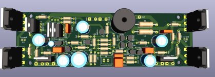
The last and final video from Michael Beeny and Ron Schauer about the L12-2 Version 5.
"The conclusion" of an apparently not recommended product.
"The conclusion" of an apparently not recommended product.
Last edited:
When I contacted LJM about the stability issue, he said that the amp was okay, but transistors A1837 and A3567 were defective. He said that they should be replaced with the same devices from any other brand. I ordered Toshiba transistors, replaced 3567 and both 1837, and got the same instability as before. Replay of LJM:.... or just buy the L12-2 to L12-4 as long as they´re available.
that amplifier requires transistors of the special brand, to work properly! WTF?! What is that trolling?LJM: There is no problem with JJAG's trademark.
Better not buy either version of those amps, have self-respect, and not feed a troll.
For me, it is just a bad design. He is simply not capable to design an amp. The more he strays from the Blameless topology, the more problems it has.
CFP can start to oscillate very easily due to very high gm. There are 2 CFP in the circuit. One is the input stage, the other is at output stage. My rule of thumb is to keep the input(base) of CFP capacitive. Also always put local power bypass caps. Unbypassed long power leads are equivalent to inductive lead presented at the input.
Here is what happens when the input of CFP is inductive.
Post in thread 'How (Not) to Make An Oscillator with Emitter Follower'
https://www.diyaudio.com/community/...tor-with-emitter-follower.421436/post-7885967
Last edited:
Hi ,
made a new pcb. But it is difficult to design without long tracks. Comments welcome....
The heatsink for 1837 is missing, i cant find such a heatsink in kicad. Changes of Mr. Beeny are in, exept the resistors at the input, have to change the value.
I think it is the form of the pcb made all difficult. The output transistors have to move more to the middle...
Any change is possible to make the amp stable....(perhaps)
Greets
Peter
Attachments
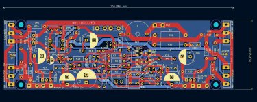
I don’t think layout changes can fix it. The circuit has to be modified first.made a new pcb. But it is difficult to design without long tracks. Comments welcome....
CFP
The scenario is not exactly witchcraft,
but some design flaws are immediately obvious, of course, but so be it. So, if I were to get the order and the customer insists on a parallel connection of the power transistors, then it might be worth starting with this approach.

And never forget that the operating voltage rails must be supported and blocked directly at the event.
Mr. Beeny
realizes this extremely important point by bridging the capacitive multiplier and thus creating a path to the two additional 1µF MKS.
Of course, the 33µF capacitor must not simply be in parallel with the Q6 - the solution has already been posted.
HBt.
The scenario is not exactly witchcraft,
but some design flaws are immediately obvious, of course, but so be it. So, if I were to get the order and the customer insists on a parallel connection of the power transistors, then it might be worth starting with this approach.
And never forget that the operating voltage rails must be supported and blocked directly at the event.
Mr. Beeny
realizes this extremely important point by bridging the capacitive multiplier and thus creating a path to the two additional 1µF MKS.
Of course, the 33µF capacitor must not simply be in parallel with the Q6 - the solution has already been posted.
HBt.
that's right 👍I don’t think layout changes can fix it. The circuit has to be modified first.
- Home
- Amplifiers
- Solid State
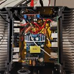
- NEW L12/2 version 5. I have just received a pair of these amplifiers, I stopped testing because the boards are unstable