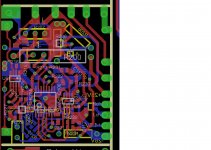
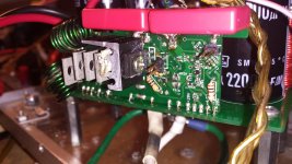
It is the same board I used before but with some modifications. Routing is done manually, there is too much for the auto router. Plus there are cut away daughter boards that fit together and have to line up with the proper connections. I will cut them apart because the boardhouse charges more for paneling and cut outs. Lots of SMD means lots of vias. With through hole you can use the pins as the vias. I did that here where applicable. Smallest via is 14mil, but that is not that small anymore. They can do 6mil now.
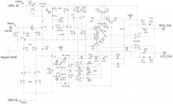
Just to show that there is a lot of different stuff going on, I have now began to commit the schematic drawings to electronic format. Here is the volume control circuit, the small daughter board at the bottom left corner of the PCB. I included component values (subject to minor change😛), and the current drawn from the supply. The 4.5V source comes from the main PCB from the logic control circuit supply.
The THAT 2162 IC requires the control ports to be low impedance. The AD8039 duel op amp (SOT23-8 package) act as input and output buffers for the THAT 2162. SW1 is a slide switch that allows two different gain settings so as to be able to interface with either a standard small signal source (1.5Vp) or a phone/i-pod nano (0.4Vp). It looks like a neat circuit, I can't wait to try it out!
The THAT 2162 IC requires the control ports to be low impedance. The AD8039 duel op amp (SOT23-8 package) act as input and output buffers for the THAT 2162. SW1 is a slide switch that allows two different gain settings so as to be able to interface with either a standard small signal source (1.5Vp) or a phone/i-pod nano (0.4Vp). It looks like a neat circuit, I can't wait to try it out!
Attachments
Last edited:
2 layer PCB, but the daughter boards build upwards.🙂 Would like 93mil thick boards but standard 62mil will suffice for prototype. There are basically two separate GNDs, power GND (dirty GND) and signal GND (clean GND). More specifically, the scheme is a star on star. This is of course to avoid GND loops.
Last edited:
Just received a quote from ETek-Net of $116 for 4 boards including shipping with 8 day lead. Not too bad, They made the last version PCBs so I expect at least the same quality.🙂
Now the fingernail chewing begins....😀
Now the fingernail chewing begins....😀
After seeing your design , I feel like a caveman.
It must be our relative distance from oak ridge 😀 . WOW !
OS
It must be our relative distance from oak ridge 😀 . WOW !
OS
Slowly but surly I am getting the schematic translated to electronic form.😛
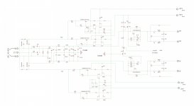
Power supply circuit.....
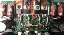
Only a single center tapped secondary is required, 38 to 42VAC. The voltage supply for the IPS and VAS circuit comes from the voltage doubler and each channel has it's own regulator circuit, all on board. The reference for the output voltage is provided by a low noise CCS consisting of a cascoded 4117 Jfet (Idss~50uA) and a MF resistor bypassed by a COG type cap. No Zeners here, Zeners are great for protection but make nasty noisy voltage sources. There are better methods.😉 Feedback is provided to one of the two J-fets forming the differential and is compared to the voltage reference. The pass transistors are 2N5087 and 2N5089 in SOT-23. Although the 2N5089 Vceo is 25V, due to the depletion properties of Jfets, the pass BJTs are always on and saturated until the doubled supply builds up above 37V so they will never see that much Vce. They do however have extraordinary hfe....>500 for 3N5089.🙂 The CSD18534KCS mosfets are Nexfets. These are the next generation of mosfets, similar to Trench fets in architecture, but have been modified to eliminate the major issue with Trench fets. Trench fets tend to have an overlapping electric field during Vds saturation between the gate and drain causing the need for significantly more charge in order to turn off the device. Consequently, Nexfets require very little gate charge to operate yet still have the very low Rds-on that Trench fets have.🙂
Power supply circuit.....
Only a single center tapped secondary is required, 38 to 42VAC. The voltage supply for the IPS and VAS circuit comes from the voltage doubler and each channel has it's own regulator circuit, all on board. The reference for the output voltage is provided by a low noise CCS consisting of a cascoded 4117 Jfet (Idss~50uA) and a MF resistor bypassed by a COG type cap. No Zeners here, Zeners are great for protection but make nasty noisy voltage sources.
There are better methods.😉 Feedback is provided to one of the two J-fets forming the differential and is compared to the voltage reference. The pass transistors are 2N5087 and 2N5089 in SOT-23. Although the 2N5089 Vceo is 25V, due to the depletion properties of Jfets, the pass BJTs are always on and saturated until the doubled supply builds up above 37V so they will never see that much Vce. They do however have extraordinary hfe....>500 for 3N5089.🙂 The CSD18534KCS mosfets are Nexfets. These are the next generation of mosfets, similar to Trench fets in architecture, but have been modified to eliminate the major issue with Trench fets. Trench fets tend to have an overlapping electric field during Vds saturation between the gate and drain causing the need for significantly more charge in order to turn off the device. Consequently, Nexfets require very little gate charge to operate yet still have the very low Rds-on that Trench fets have.🙂Attachments
Last edited:
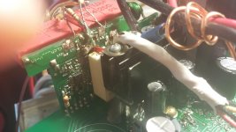
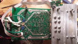
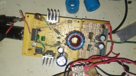
Sorry is has been slow to develop this latest design prototype update. Finding time to work on this hobby has been an issue. But anyway, everything seems to be working quite well so far. I still have a few loose ends to tie up such as attaching the fan and thermistor for the temp control circuit and a few minor adjustments.
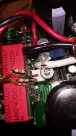
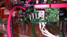
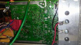
As you can see, this is a different kind of amp. Both channels' volume is adjusted by a single potentiometer that sets a control voltage for a volume control circuit based on the THAT2162 duel VCAs and a couple AD8039 duel op amps in the SOT-23(8) package. This circuit is based on the datasheet for the THAT2162 used as a stereo volume controller. This circuitry is on the daughter board with the large red WIMA 1uf PPM input caps. The signal then goes to a mixer/buffer that provides a summing node for the audio signal with the DC servo output and drives the input stage of the voltage amplifier. Each VAS circuit is powered by a small signal voltage regulator supplied by the voltage doubler circuit from the power supply section. The VAS section is a current feedback amplifier using a "complementary"🙄 J-fet IPS driving a common base VAS output. This circuit employes a common mode feedback loop to each J-fet input device in order to mitigate the difference in Gm of the N-ch vs P-ch devices. Since the common mode amplifiers work in class A, there is essentially 3 signal feedback loops. The VAS circuit output drives the very high input Z of the output stage circuit block. The output stage circuit is a bootstrapped, cascoded version of HEC using very fast EC amplifiers and general cheap planer stripe type Mosfets. The output stage bias current is really about 10mA. Typically this bias is about 200mA, but to show that it is possible to generate an error signal fast enough to fill in the missing Gm of these devices is in fact possible..... In fact, at a very low listening level, the error signal is actually larger in magnitude than the output! Also with +/-28V rails, the total bias power wasted by both channels is about 1W.😀 Each common mode loop must be freq. compensated just as the differential loop must be freq. compensated. Also the EC amplifier loops in the output stage must be freq. compensated and so must the output devices be locally compensated as well. The differential loop uses TMC compensation to provide phase lead and typical miller compensation around the amplifying devices to provide lag compensation to the VAS section. Surprisingly when I finally attached the TMC, the thing got really stable. I am thrilled.
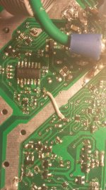
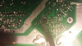
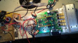
Despite using just one pair of TO-220 transistors per channel, cranking out 100W average @4R is not a problem here due to the specific mounting scheme and the devices used. I drove my Cerwin AT-10s to Xmax, nearly bottomed them out and then turned back to about 2/3 max output. The plastic package of the output devices were just a bit warm to the touch. Also on the other side of the daughter board with the red input caps is the output coils and the solid state relay circuits. Oh yeah, SSR......uh HuH!!!😎
Anyway, some recent photos.........
As you can see, this is a different kind of amp. Both channels' volume is adjusted by a single potentiometer that sets a control voltage for a volume control circuit based on the THAT2162 duel VCAs and a couple AD8039 duel op amps in the SOT-23(8) package. This circuit is based on the datasheet for the THAT2162 used as a stereo volume controller. This circuitry is on the daughter board with the large red WIMA 1uf PPM input caps. The signal then goes to a mixer/buffer that provides a summing node for the audio signal with the DC servo output and drives the input stage of the voltage amplifier. Each VAS circuit is powered by a small signal voltage regulator supplied by the voltage doubler circuit from the power supply section. The VAS section is a current feedback amplifier using a "complementary"🙄 J-fet IPS driving a common base VAS output. This circuit employes a common mode feedback loop to each J-fet input device in order to mitigate the difference in Gm of the N-ch vs P-ch devices. Since the common mode amplifiers work in class A, there is essentially 3 signal feedback loops. The VAS circuit output drives the very high input Z of the output stage circuit block. The output stage circuit is a bootstrapped, cascoded version of HEC using very fast EC amplifiers and general cheap planer stripe type Mosfets. The output stage bias current is really about 10mA. Typically this bias is about 200mA, but to show that it is possible to generate an error signal fast enough to fill in the missing Gm of these devices is in fact possible..... In fact, at a very low listening level, the error signal is actually larger in magnitude than the output!
Also with +/-28V rails, the total bias power wasted by both channels is about 1W.😀 Each common mode loop must be freq. compensated just as the differential loop must be freq. compensated. Also the EC amplifier loops in the output stage must be freq. compensated and so must the output devices be locally compensated as well. The differential loop uses TMC compensation to provide phase lead and typical miller compensation around the amplifying devices to provide lag compensation to the VAS section. Surprisingly when I finally attached the TMC, the thing got really stable. I am thrilled.Despite using just one pair of TO-220 transistors per channel, cranking out 100W average @4R is not a problem here due to the specific mounting scheme and the devices used. I drove my Cerwin AT-10s to Xmax, nearly bottomed them out and then turned back to about 2/3 max output. The plastic package of the output devices were just a bit warm to the touch. Also on the other side of the daughter board with the red input caps is the output coils and the solid state relay circuits. Oh yeah, SSR......uh HuH!!!😎
Anyway, some recent photos.........
Attachments
-
 gg.jpg301.9 KB · Views: 130
 -
 gg (6).jpg327.2 KB · Views: 137
 -
 gg (10).jpg395.4 KB · Views: 117
 -
 gg (14).jpg328.2 KB · Views: 116
 -
 gg (13).jpg319.2 KB · Views: 128
 -
 gg (12).jpg393.4 KB · Views: 137
 -
 gg (11).jpg359.5 KB · Views: 128
 -
 gg (9).jpg546.1 KB · Views: 152
 -
 gg (7).jpg480.2 KB · Views: 247
 -
 gg (8).jpg635.6 KB · Views: 290
Last edited:
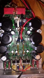
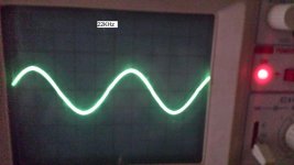
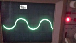
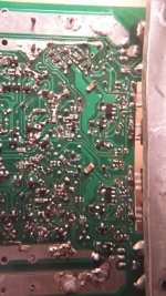
Photos of the bottom side. Also the output and error signals. I noticed that the error signal changed in magnitude as I did a frequency sweep. It increased at the low end, and as frequency increased, the error got smaller, and then larger. Also it varied in phase. This is a reflection of the changing speaker Z vs frequency. I guess this means that as far as the speaker is concerned, it sees a very close approximation of a true voltage source at the output node. This is good, no? 🙂 Yes, very good. The sound is very clear and the highs and sound stage perception is surprisingly precise. This amp does not care to have surround sound speakers connected in series +-/-+ between the two channel's outputs so as to play the difference between left and right at opposite phase. The EC signal reacts accordingly.😎
The sound is very clear and the highs and sound stage perception is surprisingly precise. This amp does not care to have surround sound speakers connected in series +-/-+ between the two channel's outputs so as to play the difference between left and right at opposite phase. The EC signal reacts accordingly.😎Attachments
-
 gg (18).jpg300.8 KB · Views: 118
 -
 20150824_193951.jpg298 KB · Views: 109
 -
 gg (19).jpg281.1 KB · Views: 119
 -
 gg (20).jpg284.9 KB · Views: 116
 -
 gg (4).jpg472 KB · Views: 117
 -
 gg (3).jpg456.1 KB · Views: 107
 -
 gg (2).jpg268.5 KB · Views: 122
 -
 gg (16).jpg1,006.7 KB · Views: 134
 -
 gg (17).jpg519.7 KB · Views: 115
 -
 gg (15).jpg441.1 KB · Views: 118
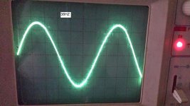
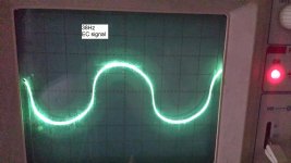
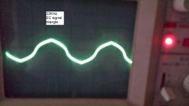
Here is the EC signal at 22KHz triangle wave output. 🙂
Also the power transformer used. Some amps have issues with being powered by a transformer with a very low Z. This one is a 1400VA toroid. There does not seem to be any issues with using this transformer although it IS a bit of overkill.😛
Also the power transformer used. Some amps have issues with being powered by a transformer with a very low Z. This one is a 1400VA toroid. There does not seem to be any issues with using this transformer although it IS a bit of overkill.😛
Attachments

One cool thing I forgot to mention is that the large power resistor that feeds the +5V source for the input volume control circuit is 180R 5W. It has to do about 3.5W maximum and this is when the volume is set at minimum. The control pins of the THAT2162 require low Z drive. However, I have managed to place it so as it is in contact with the small heat sink for the power rectifiers. It turns out that when the volume is minimum, the resistor dissipates the most heat but the rectifiers are at minimum dissipation. But when the volume is cranked, the opposite occurs and everything more or less balances out.😀
There will be more on this project to come.............😉
PS: Dang it! But I did buy the wrong fuses......these holders are for ATM, not ATC. Had to manipulate and trim the blades of the fuses to fit, looks kinda ugly.
There will be more on this project to come.............😉
PS: Dang it! But I did buy the wrong fuses......these holders are for ATM, not ATC. Had to manipulate and trim the blades of the fuses to fit
, looks kinda ugly.
Last edited:
CBS, I've been following your work with great interest for the past three years & look forward to further info. I took your idea for the voltage doubler feeding reg for the boosted rails on some of my Hexfet projects and this works very well.
Cool. I've been using that idea for a long time, even with bipolar outputs. I like to cascode VAS😉.
When it comes to mosfet outputs, particularly verticals, bootstrapping the driver stage also is a viable option that I find works very well, especially with HEC gate drive circuit.
When it comes to mosfet outputs, particularly verticals, bootstrapping the driver stage also is a viable option that I find works very well, especially with HEC gate drive circuit.
The VAS in the amplifiers for this circuit (stereo😀) is a common gate J-fet amplifier with a floating cascode. Last model used bipolar VAS, but the model before that used J-fet VAS and hands down the J-fet is much better sounding for sure and so used in this one. But I needed to stack the J-fet cascodes to handle peak voltage, like 70V. Using 40V J-fet, much above 30V Vds and the shape of the field inside J-fet begins to become misshapen causing distortions.
The outputs are planer stripe devices, variation of first generation mosfet. Very rugged. Although very non-linear at a bias of 25mA, the local error correction driver stage is really truly amazing. 🙂
The outputs are planer stripe devices, variation of first generation mosfet. Very rugged. Although very non-linear at a bias of 25mA, the local error correction driver stage is really truly amazing. 🙂
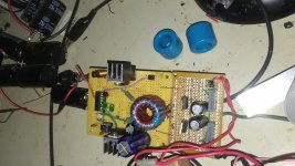
Huge difference with this circuit from the last is the power supply used. For now it is a 12V SMPS step up circuit like a car amp supply. The transformer core is slightly undersized but I have others or use multiple cores. Anyway, caps are shrunk at 60Khz instead of 60Hz.🙂 controller is SG3525
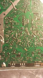
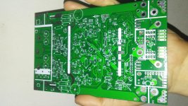
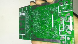
And also pics of PCB. It is a 4-layer board. Cut outs for daughter boards are marked in silk screen.
And also pics of PCB. It is a 4-layer board. Cut outs for daughter boards are marked in silk screen.
Attachments
first time I look at this thread .... I saw brass shims in the heatsink construction .... beware of these brass shims .... brass is not a good performer for heat transfer ....
I found a thermal conductivity table ....
Thermal Conductivity of Metals
silver 407, copper 386, gold 315, beryllium 218, aluminium 204, brass 111, bronze 26
Thermal Conductivity of Metals
silver 407, copper 386, gold 315, beryllium 218, aluminium 204, brass 111, bronze 26
- Status
- Not open for further replies.
- Home
- Amplifiers
- Solid State
- New home brew amp module