Hmm
I have told I don't want to use IRS29xxx like amplifier ClassD, but IR2110 or other(gate driver) is OK, and welcomed!
So any kind of advice with ANY gate driver(s) will be appreciate!
I don't have in Romania Micrometals cores, and Farnell(who's ok for me) doesn't import it to order it from them..
So, I must use Gendalex cores that I have and maybe later, after I will develop entire schematic and adjustments, I will try ferrite gapped cores.
Can anyone do some modificatioms to replace all after LM 361, to have only N-Mos output devices,keeping the fullbridge configuration?
with such cores you won't get any performances. try to use T106-2, Micrometals (da-mi PM si iti trimit eu kteva)
IRS2092 is a better solution than the discrecte one. you can't do a good Class D amp with discrete parts unless you make a very tight an well designed layout, on multilayer PCB.
IRS2092 is a better solution than the discrecte one. you can't do a good Class D amp with discrete parts unless you make a very tight an well designed layout, on multilayer PCB.
with such cores you won't get any performances.
Why? Do you know that cores? I couldn't find that (or any similar) part number, but they say its molibdenium-permalloy, so there is a chance for it to be usable.
DjLeco!
If IR2110 is OK, then what is the problem with IRS20957?
Pafi said:
Why? Do you know that cores? I couldn't find that (or any similar) part number, but they say its molibdenium-permalloy, so there is a chance for it to be usable.
DjLeco!
If IR2110 is OK, then what is the problem with IRS20957?
I'm intending to use IR as gate driver only, somethink like here (looks simplified)
An externally hosted image should be here but it was not working when we last tested it.
But I must take care about deadtime...
That IRS looks OK do you have some schematics?
I'm intending to use IR as gate driver only,
And as level shifter, aren't you?
That IRS looks OK do you have some schematics?
It's on the datasheet!
Be careful, the linked schematic is faulty!
cnx said:with such cores you won't get any performances. try to use T106-2, Micrometals
You have PM.
I'm interesed to buy some micrometals cores.
Pafi said:Be careful, the linked schematic is faulty! [/B]
I know, I'd just give it like an example...
Presuming that the deadtime part is ok,with some R/C to ground on inputs of IR circuit, is ok to conect Hi in of Hi side with Low in of the Low side driver, same for other input?
Like in Yorkville bridged active subwoofer amplifier?
Wich are the best mos fets for 125 Khz class D bass only, amplifier?
Please share to me!
Presuming that the deadtime part is ok,with some R/C to ground on inputs of IR circuit,
I don't know how do you intend to do it, but be careful! IR2110 inputs are referenced to negative rail, so you can't connect them directly to the comparator, if you use symmetrical supply voltage! Level shifter needed! (Wich is present in IRS20957, just like dead time circuit, that's why I suggested it.)
is ok to conect Hi in of Hi side with Low in of the Low side driver, same for low in?
I repeat: your terminology is wrong! Make your life easier by follow the conventions: low side means the parts connected to the negative rail, high side means the positive rail!
Otherwise yes, you can connect low in of inverting channel to the Hi in of noninverting channel, and vica versa, however there are better methods too. (3-level modulation.)
The best FET? It depends on what is available for you, for what price, and the power demand. (And depends on topology too, for example BCA amps needs different parameters.)
Some good FETs in 150 V class:
FDP2552, IRFB4321
Pafi [/i]][/QUOTE] [B]IR2110 inputs are referenced to negative rail said:Use this configuration for the best results - opto/driver/floating smps. It is best for versatility, construction, hard clipping, etc.
Also, you can use EE 3f3 gapped (easy to find). Dont ignore deadtime and feedback construction.
Ionut, some drawings will be very appreciate, I don't understand nothing with those pcb's...
Also, don't forget, I want to use in FULLBRIDGE topology!
Waiting for some schematic ideeas with some fastest HCPL's optos!
I use LM361 high comparator, wich have balanced outputs, very helpfull for bridging topology!
Ne putem intilnii pe un messenger yahoo?
claudiu971 este al meu id.
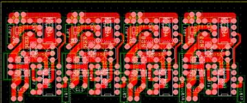
6n137 is enough. Use lm361, but insert logic gates with deadtime function (also shutdown is easy to implement in this stage), drive opto-driver TC429 (6A capability, inverting), drive mosfet. You will see in the photo attached an configuration for 4 modules (full bridge or stereo). Also, dont use paralell mosfets if you intended to work full range. Remember for continuos ground plane on the top of pcb.
DjLeco!
Then it's OK, however feedback will be a little more complicated, but over the R/C you will need 1-1 diodes also for dead-time generation.
3 level modulation (simplified!):
http://users.hszk.bme.hu/~sp215/elektro/eszosztas/3 level PWM.gif
This way you get twice as much effective frequency on output, and much lower output ripple, or you can use much smaller (=higher freq) output filter.
the GND part of it will be common with -Vcc part of final stage.
Then it's OK, however feedback will be a little more complicated, but over the R/C you will need 1-1 diodes also for dead-time generation.
3 level modulation (simplified!):
http://users.hszk.bme.hu/~sp215/elektro/eszosztas/3 level PWM.gif
This way you get twice as much effective frequency on output, and much lower output ripple, or you can use much smaller (=higher freq) output filter.
Pafi said:DjLeco!
Then it's OK, however feedback will be a little more complicated, but over the R/C you will need 1-1 diodes also for dead-time generation.
Sure, I ommited to write about it, my blame...
3 level modulation (simplified!):
http://users.hszk.bme.hu/~sp215/elektro/eszosztas/3 level PWM.gif
I don't really understand a big thing from there, could be more specific, with some really schematic?
I repeating I don't need to push more than 125 Khz switching because I intend to use only in 20-300Hz band, not fullrange.
For Mid-Hi I will always use Class AB+B no more of 500W Rms/8 ohms.
.
Thank you for reply,also Ionut, I will give a try too.
I don't really understand a big thing from there, could be more specific, with some really schematic?
A more complicated schematic doesn't help. The goals are:
- smaller output choke
- higher efficiency
- better quality
If you want to understand the benefits, you have to calculate filter, feedback, etc...
On PC main boards you can see multiphase (multi-level) SMPSs for CPU, however there is only DC output.
ionutgaga said:6n137 is enough. Use lm361, but insert logic gates with deadtime function (also shutdown is easy to implement in this stage), drive opto-driver TC429 (6A capability, inverting), drive mosfet. You will see in the photo attached an configuration for 4 modules (full bridge or stereo). Also, dont use paralell mosfets if you intended to work full range. Remember for continuos ground plane on the top of pcb.
Are the 6N137's fast enough? Crown BCA uses them (Fairchild's version, but it's the same) , but rise/fall times aren't as important with BCA. It solves a WHOLE LOT of problems when running full bridge and if you're willing to use little auxiliary supplies (which I would be, I have a box of 24 of those little split-tans for similar purposes).
Why wouldn't you parallel mosfets? It may be the only way to get source inductance low enough if you're trying to drive 140A peak currents. For a design I'm starting, I was planning 12 in parallel per bank. The 6N137's and driver circuits on isolated supplies would make life easier driving all that. Clock frequency is still TBD. It's just for subs and will be in a shootout with 4-step class H. Whichever ends up being more manufacturable gets duplicated 4 times.
If you wanted to implement deadtime in the logic end of it would an HC123 monostable and a pair of flip-flops do the trick? I'm thinking adjust one pot to tweak it right in to whatever you want.
To do something big, I'm thinking it will take 4 layers. Two alternating planes for the H-bridge, ground, and logic/audio on top. And for the cheapskate who doesn't want to do a $1000 board run on EACH REV, that's two separate PCBs sandwiched 🙂.
6N137 (or HCPL0600 for SMD) is fast enough for most applications, in practice it introduces approx. 50ns delay both for rising and falling edges.
With IR2110 and similar drivers with separate HIN and LIN inputs, dead time adjustment (pulse shortening, or sometimes pulse extension) does not require extra gates, just RCD networks on the input pins of the driver. I like to use two XOR gates to generate the HIN and LIN signals without propagation delays between them.
Otherwise, conventional gates (74HC00, 74HC04) or schmitt-triggered buffers (74HC14) may be used. I also like to use a minimum pulse width generator, which is easily implemented with four NAND gates and two RCD.
BTW: My current project does +/-70A peak and up to +/-170V (only limited by supply sag) with just 8 MOSFET (5KW on 2 ohm short term). Prototypes are already being beta tested by final customers. Paralleling MOSFET is a double-edged sword, as Rds-on is reduced but gate charge and capacitances rise quickly, not to mention layout complexity... The MOSFET with the lowest Rds-on to output capacitance and gate charge ratio should be used.
Yes
I will repeat again,ONLY FOR BASS 20Hz-300Hz use.
125 Khz are more than enough.
I think 6N137 will be fast enough for 125 Khz what I intend to use.
BTW, can anyone do some schematic drawings with full bridge confuguration of 4 pieces of N-Mos-Fet output devices, drived by optocuplor and Mos-Fet driver, wich receive signal from both 9 and 11 balanced outputs of LM361 IC,PLEASE?
My schematic use National's LM361 Hi-Speed comparator and I want to use both 9 and 11 balanced outputs for bridged topology.
Oficially my schematic are is in fullbridge, but is with discrete transistors for mosfet drivers and uses P+N MosFets on output.
I'm intending do modifications to use ONLY N MosFets, during poor P-Mos transistors parameters...
I own both type of non inverting and inverting optos, HCPL2611 and TLP2601 wich are used by Crown BCA Amps, also TC4421 and TC4422 MosFet Drivers and also MC34151 Inverted Driver.
Can anyone make some drawings?
Here is 2 small modules with IRF540 and IR2110 with series deadtime network on Hi and Low inputs of IR 2110; ,270 ohms with 330 pf to ground and 1n4148 with 47 ohms(unmounted yet) on 270 ohms parraleled .
I'm waiting for your advices and maybe some drawings.
Feedback is not a problem, I'm ok with that.
Thank all of you alot for possible support!
and closer look:
All components useh here are intended for testing only!
I will repeat again,ONLY FOR BASS 20Hz-300Hz use.
125 Khz are more than enough.
I think 6N137 will be fast enough for 125 Khz what I intend to use.
BTW, can anyone do some schematic drawings with full bridge confuguration of 4 pieces of N-Mos-Fet output devices, drived by optocuplor and Mos-Fet driver, wich receive signal from both 9 and 11 balanced outputs of LM361 IC,PLEASE?
My schematic use National's LM361 Hi-Speed comparator and I want to use both 9 and 11 balanced outputs for bridged topology.
Oficially my schematic are is in fullbridge, but is with discrete transistors for mosfet drivers and uses P+N MosFets on output.
I'm intending do modifications to use ONLY N MosFets, during poor P-Mos transistors parameters...
I own both type of non inverting and inverting optos, HCPL2611 and TLP2601 wich are used by Crown BCA Amps, also TC4421 and TC4422 MosFet Drivers and also MC34151 Inverted Driver.
Can anyone make some drawings?
Here is 2 small modules with IRF540 and IR2110 with series deadtime network on Hi and Low inputs of IR 2110; ,270 ohms with 330 pf to ground and 1n4148 with 47 ohms(unmounted yet) on 270 ohms parraleled .
I'm waiting for your advices and maybe some drawings.
Feedback is not a problem, I'm ok with that.
Thank all of you alot for possible support!
An externally hosted image should be here but it was not working when we last tested it.
and closer look:
An externally hosted image should be here but it was not working when we last tested it.
All components useh here are intended for testing only!
We can give you many hints but no one of us is likely to do your homework 😉
If you want to do a good class D amplifier you have to do some research on:
- Ground/power planes and how to implement them with double sided PCB
- Supply decoupling, capacitor parasitics, how to parallel capacitors the right way and how to obtain non-resonant supply rails
- MOSFET package parasitics, and how to tame the resulting resonance with one or more RC snubbers
- How to choose cores and wind inductors for a given inductance and saturation current
- Modulators: Triangle wave or self oscillating? And how to do basic simulation of them to adjust frequency compensation, get an idea of frequency response, etc...
Most of that information may be found by searching through the forum (lots of patience and intuition required).
Eva
Eva, how I wrote, I have entire schematic,is deja in fullbridge,but oficially it uses P-Mos and N-mos for output devices, drived by discrete transistors, as you can see on attachment on first page of this thread.
Is an MC14060 oscillator with 4 Mhz ceramic resonator,with an operational and a transistor wich gives me 125 Khz triangle signal.
Also is an operational for input, other for positive and negative feedback, another for summing and DC offset and the LM361 comparator, with their positive and negative outputs connected to schematic that I attached on first page (driver and final mosfets).
What I need is JUST to replace all output part,with Nmos fets,I want to keep everything for what I described,and the final mosfets become all NMos, not PMos+NMos, how they are now...
No need indications for PCB construction or other stuff, just what I asked.
I just need final stage with Nmos transistors, in fullbridge configuration, drived by IR2110 or opto+mos driver.
The
Can anybody help me ?
You can find sample N-channel schematics with IR gate drivers everywhere, but a class D output stage is much more than a schematic. You have to do the layout, and do it properly, tame the resonances, etc...
- Status
- Not open for further replies.
- Home
- Amplifiers
- Class D
- New ClassD project Starting from 0