Recently finished rereading Linearaudio Volume 2 where Jan Didden published Samuel Groner's article "A New Amplifier Topology with Push-Pull Transimpedance Stage".
This wonderfully written article explains how to implement folded cascodes in both the Transconductance VI converter and Transimpedance IV converter.
I am impressed with the possibilities of folded cascodes since I built Salas Folded simplistic phono.
With proper implementation, the folded cascode tech can increase circuit PSRR by referencing the input of the transimpedance stage to GND instead to one of the voltage rails.
So following Gronner's design I implemented the topology into a high power lateral mosfet power amp.
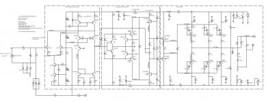
Please have a look at the simulation below...
Now I will explain the circuit so everyone can follow my reasoning....
IPS - transconductance stage:
J1 and J2 form the typical long tailed pair
Q4 Q6 R23 D17 and D18 form the CCS that sets 4mA in each R26 R27 degeneration resistors. (These are set to 100ohm for improving input stage distortion and slew rate)
Q11 Q12 form the IPS folded cascode
To increase gain, the folded cascode is loaded by twin CCS formed by Q9 Q10.
This CCS must provide 8.5mA so the folded cascode Q11 Q12 works with 4.3mA (slightly higher than the LTP current)(If the folded cascode current is lower than what is used in the LTP, additional distortion at high freq might result because at peak output currents of the IPS diff pair, the folded cascode transistors will switch fully off)
Emitter resistors of the current mirror R54 R55 should have a large value to minimise the noise contribution of the current mirror.... As large emitter resistors will introduce a pole in the open loop gain of the amplifier, two capacitors C14 C29 are placed in parallel with the emitter resistors.
Q13 is a common base transistor used to keep the folded cascode transistors Q11 Q12 at approximately the same collector emitter voltage minimizing offset due to early effect. The base current of Q13 also cancels the base current errors in the current mirror also reducing offset.
Finally the differential signal is converted into single ended by the works of the current mirror formed by Q14 and Q32.
Transimpedance stage:
It is arranged as complementary push-pull configuration so to have a better slew rate response.
Voltage from Q22 emitter to Q23 emitter provides bias for the common emitters Q25 Q26.
R48 R51 emitter resistors are needed to reduce sensitivity to transistor tolerances and thermal effects. Minimizing the value of these resistors is preferable as this lowers the sensitivity to loading of the second stage output node so we should choose their value for a vdrop of < 100mV.
Once these are determined, bias voltage for Q25 Q26 is found through the choice of R25 R39.
Current on the emitter followers Q22 Q23 is set with R46 R47.
The collector current of the folded cascodes Q28 Q29 is set both by the emitter resistors R52 R56 and the base reference voltages set by D3 D7.
Capacitor C38 linking the emitters of the folded cascode is useful to increase transient output currents.
Current limiting:
Q24 Q27 limit the collector current of the common emitters Q25 Q26 to six times the quiescent current.
Simulation predicts that in overload conditions the collector current of Q25 Q26 might increase beyond the maximum ratings of these transistors.
This wonderfully written article explains how to implement folded cascodes in both the Transconductance VI converter and Transimpedance IV converter.
I am impressed with the possibilities of folded cascodes since I built Salas Folded simplistic phono.
With proper implementation, the folded cascode tech can increase circuit PSRR by referencing the input of the transimpedance stage to GND instead to one of the voltage rails.
So following Gronner's design I implemented the topology into a high power lateral mosfet power amp.
Please have a look at the simulation below...
Now I will explain the circuit so everyone can follow my reasoning....
IPS - transconductance stage:
J1 and J2 form the typical long tailed pair
Q4 Q6 R23 D17 and D18 form the CCS that sets 4mA in each R26 R27 degeneration resistors. (These are set to 100ohm for improving input stage distortion and slew rate)
Q11 Q12 form the IPS folded cascode
To increase gain, the folded cascode is loaded by twin CCS formed by Q9 Q10.
This CCS must provide 8.5mA so the folded cascode Q11 Q12 works with 4.3mA (slightly higher than the LTP current)(If the folded cascode current is lower than what is used in the LTP, additional distortion at high freq might result because at peak output currents of the IPS diff pair, the folded cascode transistors will switch fully off)
Emitter resistors of the current mirror R54 R55 should have a large value to minimise the noise contribution of the current mirror.... As large emitter resistors will introduce a pole in the open loop gain of the amplifier, two capacitors C14 C29 are placed in parallel with the emitter resistors.
Q13 is a common base transistor used to keep the folded cascode transistors Q11 Q12 at approximately the same collector emitter voltage minimizing offset due to early effect. The base current of Q13 also cancels the base current errors in the current mirror also reducing offset.
Finally the differential signal is converted into single ended by the works of the current mirror formed by Q14 and Q32.
Transimpedance stage:
It is arranged as complementary push-pull configuration so to have a better slew rate response.
Voltage from Q22 emitter to Q23 emitter provides bias for the common emitters Q25 Q26.
R48 R51 emitter resistors are needed to reduce sensitivity to transistor tolerances and thermal effects. Minimizing the value of these resistors is preferable as this lowers the sensitivity to loading of the second stage output node so we should choose their value for a vdrop of < 100mV.
Once these are determined, bias voltage for Q25 Q26 is found through the choice of R25 R39.
Current on the emitter followers Q22 Q23 is set with R46 R47.
The collector current of the folded cascodes Q28 Q29 is set both by the emitter resistors R52 R56 and the base reference voltages set by D3 D7.
Capacitor C38 linking the emitters of the folded cascode is useful to increase transient output currents.
Current limiting:
Q24 Q27 limit the collector current of the common emitters Q25 Q26 to six times the quiescent current.
Simulation predicts that in overload conditions the collector current of Q25 Q26 might increase beyond the maximum ratings of these transistors.
Attachments
Last edited:
Now I will explain the circuit so everyone can follow my reasoning....
IPS - transconductance stage:
J1 and J2 form the typical long tailed pair
Q4 Q6 R23 D17 and D18 form the CCS that sets 4mA in each R26 R27 degeneration resistors.
Q11 Q12 form the IPS folded cascode
To increase gain, the folded cascode is loaded by twin CCS formed by Q9 Q10.
This CCS must provide 8.5mA so the folded cascode Q11 Q12 works with 4.3mA (slightly higher than the LTP current)
Finally the differential signal is converted into single ended by the works of the current mirror formed by Q14 and Q32.
I will come back with more information regarding biasing and resistor values choices.
I'd worry about the lack of protection components on the gates of the output devices if you build this for real. The source resistors aren't required with laterals, but here would enable current sharing to be measured/checked, and ameliorate differences between parallel devices.
Hi Mark
If you mean the protection diodes I did not include them for sim purposes... tomorrow I will post a completed schematic 🙂
If you mean the protection diodes I did not include them for sim purposes... tomorrow I will post a completed schematic 🙂
Last edited:
Im sure they are different but hmm, sort of reminds me of Keantoken’s Aurum-X, based on Goldmund... JFET front end, and 3 pairs of Exicon latFETs on output.
I'd worry about the lack of protection components on the gates of the output devices if you build this for real. The source resistors aren't required with laterals, but here would enable current sharing to be measured/checked, and ameliorate differences between parallel devices.
Doesn't the negative temp coefficient of laterals help to balance the current draw?
The transconductance input stage and the following diamond are implemented in AD844 . I did the same topology in CFA ,BJT Unusual amp from 1987.
Please see post Slewmaster - CFA vs. VFA "Rumble" and afterwards !
Also see A New Topology For A Current Feedback Amplifier
Also see A New Topology For A Current Feedback Amplifier
Last edited:
Similar, but with an opamp:
Opamp based Amp with current driven VAS
I have build it and it works, but still heavy oscillations, when increasing bias.
Opamp based Amp with current driven VAS
I have build it and it works, but still heavy oscillations, when increasing bias.
Thank you for your comments.
I updated the first post with some considerations regarding biasing of the amplifier.
Please find below the final schematic with the gate protection diodes for the output buffer.
I updated the first post with some considerations regarding biasing of the amplifier.
Please find below the final schematic with the gate protection diodes for the output buffer.
Attachments
Im sure they are different but hmm, sort of reminds me of Keantoken’s Aurum-X, based on Goldmund... JFET front end, and 3 pairs of Exicon latFETs on output.
Thank you for the schematic.
Although it is a rather different design there are some ideas I will have the pleasure to implement.

Phase margin looks good although there is a nitid pole near 10MHz.
This pole is smoothed by the use of feed-forward capacitors C19 C37 in the emitter followers of the second stage Q22 Q23.
The emitter followers are bypassed at high frequencies so local Miller loop is a cascade of common emitter Q25 Q26 and common bases Q28 Q29, reducing the risk of instability.
This pole is smoothed by the use of feed-forward capacitors C19 C37 in the emitter followers of the second stage Q22 Q23.
The emitter followers are bypassed at high frequencies so local Miller loop is a cascade of common emitter Q25 Q26 and common bases Q28 Q29, reducing the risk of instability.
Attachments
Hi Ricardo
I hope to see it assembled and real square wave test (step test or the name people use to test with square wave) with resistive load to see real amplifier behavior.
Usually all projects now do not go to products and real tests. It is expensive and take a lot of time and need reliable test equipment($$$$$).
XRK971 do not test his board and I suppose he is waiting some one to pay his boards and do this job for him.
After bench test you can go to listening test with quality gear around amplifier and see real audio results.
Regards
Last edited:
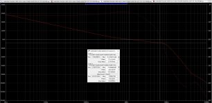
Before I start collecting parts and laying out the pcb I need some input from you guys principally regarding the FFT simulation.
Is 8 dB a bit tight for the gain margin? Or are you betting on the generous phase margin to mitigate this?
Also, are the source resistors on OPS needed when using lateral mosfets? Are these added just to assist with setting the bias? Would removing these help to cleanup some of the higher order harmonics on the FFT?
Regarding running the FFT in LTSPice, I've noted that I need a very long settling time to get a FFT plot that is stable. Like 3 to 5 seconds. Takes long to run (up to an hour), but it looks very different that plots with only a few cycles of delay. The THD doesn't really change, just the FFT plot.
Last edited:
Ricardo
If your major concern is based in THD simulation result you miss some very interesting tests in your simulation file (just the square wave test).
If you are looking only for the best distortion result or fase margem you are going wrong way (you are missing important facts).
This is why lots of people say here the best amp do not have near zero distortion - other wrong concept (good amplifier must be near of ideal OpAmp).
Good amplifier must have perfect square wave answer. Just remember Fourier in College.
Regards
Ronaldo
Last edited:
- Home
- Amplifiers
- Solid State
- New amplifier topology with laterals