Need some advise on a LTP input stage.
Hi all,
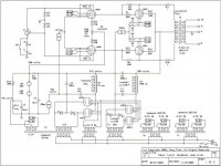
I have attached a plan for two different LTP phase splitter input stages. The idea is to hang the whole of the input stage off of a -300V negative rail. I am having some real difficulty conceptualising all of the issues involved so I have a few questions. the LTP is expected to draw about 10mA (20mA for two channels) so it should be possible to create a very stable neg supply with a simple CLC filter. The intention is to go with the pentode version, the triode version is just there to illustrate the basic concept.
1- In the first triode based schematic is the bottom resistor functioning to extend the tail of the LTP, or is it just burning up voltage.
2- In the second schematic will the voltage across R10 stay stable and so not effect the screen voltage.
3- If I substitute a CCS for R10 in the second scheme, how will it find its own anode voltage, and again will that voltage stay stable.
Am I barking up the wrong tree. Are there any issues I have failed to spot.
Shoog
Hi all,
I have attached a plan for two different LTP phase splitter input stages. The idea is to hang the whole of the input stage off of a -300V negative rail. I am having some real difficulty conceptualising all of the issues involved so I have a few questions. the LTP is expected to draw about 10mA (20mA for two channels) so it should be possible to create a very stable neg supply with a simple CLC filter. The intention is to go with the pentode version, the triode version is just there to illustrate the basic concept.
1- In the first triode based schematic is the bottom resistor functioning to extend the tail of the LTP, or is it just burning up voltage.
2- In the second schematic will the voltage across R10 stay stable and so not effect the screen voltage.
3- If I substitute a CCS for R10 in the second scheme, how will it find its own anode voltage, and again will that voltage stay stable.
Am I barking up the wrong tree. Are there any issues I have failed to spot.
Shoog
Attachments

Your using an input transformer to split the phase. There is no need for the negative supply, or a long tail. Just have the two tubes still share a cathode bias resistor. Ground makes a better voltage reference than a negative supply. So it would be better to bump up the B+ and drop the - supply, if your circumstance permits. Personally, I'd replace V4 with a capacitor, it's the lesser of two evils. Also, you may get better results hooking it to the -250 rather than -300 if keeping the bipolar power supply.
Unfortunately the need for such a large negative rail is because the anode loads on the triodes/pentodes are taken off the anodes of the output stage (ala plate to plate feedback). Pushing the +B up means achieving the same result, but with much more heat generated in the cathodes of the output stage. This scheme is less wasteful - if it works.
Unfortunately this will result in the tail been shortened to accommodate the extra current through V4, also there is the possability that the voltage over R10 will become less stable - though this shouldn't matter that much as the reference point should become more stable. I had hoped to use one VR150 for both channels.
Shoog
Also, you may get better results hooking it to the -250 rather than -300 if keeping the bipolar power supply.
Unfortunately this will result in the tail been shortened to accommodate the extra current through V4, also there is the possability that the voltage over R10 will become less stable - though this shouldn't matter that much as the reference point should become more stable. I had hoped to use one VR150 for both channels.
Shoog
What is it going to be driving? Pentodes can put out a lot of swing with just that 350V supply.
If you must have 450V total you may want to consider using a separate low current, high voltage transformer for that stage. You can usually find some small open bracket ones that are small enough to fit in the chassis. If what you are doing is getting your + and - off the same transformer. Make sure your using a CT transformer and using the two diode Full wave config for your + and another two diode Full wave for the -. That's the only way I know to pull off that asymmetrical load with getting minimal mechanical hum.
You don't need the tail anyways, And if you use a cap insted of V4 you won't have the extra DC current to sink. The - rail can be filtered down to -250 instead of -300.
Shoog said:Unfortunately the need for such a large negative rail is because the anode loads on the triodes/pentodes are taken off the anodes of the output stage (ala plate to plate feedback). Pushing the +B up means achieving the same result, but with much more heat generated in the cathodes of the output stage. This scheme is less wasteful - if it works.
Too high and unstable output resistance for a parallel feedback. Get more swing from the tranny and use cathode followers instead.
If you must have 450V total you may want to consider using a separate low current, high voltage transformer for that stage. You can usually find some small open bracket ones that are small enough to fit in the chassis. If what you are doing is getting your + and - off the same transformer. Make sure your using a CT transformer and using the two diode Full wave config for your + and another two diode Full wave for the -. That's the only way I know to pull off that asymmetrical load with getting minimal mechanical hum.
Thats exactly how I intended to derive that neg rail.
The whole question of swing is massively complicated by the plate to plate feedback arrangement. Since the DC for the pentode's needs to come through the load/feedback resistor you need a lot of voltage in order to be able to keep the feedback resistor reasonably large. Swing is really not the issue, current to the drivers is. In this case the 400V across the resistor with 5mA of current gives a feedback/load resistor of 80K, which is on the lower limit of what is acceptable without loading down the driver.
Shoog
Too high and unstable output resistance for a parallel feedback. Get more swing from the tranny and use cathode followers instead.
I have built a SE configuration of this concept (the RH807) and though I didn't much like the result, output resistance didn't strike me as been the issue.
Essentially this is a proven concept (Gary Pimms Tabor amp) I'm trying to simplify his excellent design. I may not succeed, but I don't think it will be for the reason you suggest.
Shoog
Is the intention direct coupling to the output stage? I've often wondered about using equivalant topologies that way.
Is the intention direct coupling to the output stage? I've often wondered about using equivalant topologies that way.
The Tabor amp is direct coupled. I had given up on the idea of direct coupling for the sake of simplicity, but the voltages are so near that I think I may just try to get it to work that way.
Shoog
Shoog said:
I have built a SE configuration of this concept (the RH807) and though I didn't much like the result, output resistance didn't strike me as been the issue.
Essentially this is a proven concept (Gary Pimms Tabor amp) I'm trying to simplify his excellent design. I may not succeed, but I don't think it will be for the reason you suggest.
Shoog;
output resistance of the driver does not need to satisfy you; it needs to satisfy a low input resistance of the output stage with parallel feedback by voltage. If your driver had low output resistance amplification factor of the output stage will depend on plain linear resistors; but in your case it is determined by one feedback resistor and output resistance of your driver that is not linear.
MS Windows is a proven concept (Bill Gates et all), you may try to simplify his excellent design, but what really helped them, was design of DEC team that developed NT concept to replace what Microsoft did before...
There is a lot to learn about this complicated subject. The fist stage needs to have high Rp (because it forms the lower leg of a voltage divider with the FB resistor being the upper leg) and high Gm (because it's being used as a voltage-to-current converter), so a pentode is the obvious choice. The John Broskie article in Tubecad explains how it works and the difficulties that have to be overcome, but you may need to read it thoroughly, several times, before you understand it. (I'm not 100% sure that the whole article is practical).
I've tried modeling the 'Partial Feedback' approach using LTSpice and even with a negative rail, I found that the first stage always ended up being either current-starved or voltage-starved. I gave up trying to get it working but I hope you'll be more successful!
I've tried modeling the 'Partial Feedback' approach using LTSpice and even with a negative rail, I found that the first stage always ended up being either current-starved or voltage-starved. I gave up trying to get it working but I hope you'll be more successful!
Shoog said:See the original idea.
Shoog
Yep, R5 and Ri of 6AU6 determine amplification factor of the output stage. Non-linear and variable (aging, temperature, filament voltage variations, different tubes) Ri is in the equation.
Also, there are couple of more elements: Ri of another 6AU6 and R15.
Yep, R5 and Ri of 6AU6 determine amplification factor of the output stage. Non-linear and variable (aging, temperature, filament voltage variations, different tubes) Ri is in the equation.
Also, there are couple of more elements: Ri of another 6AU6 and R15.
I have tremendous respect for Gary Pimm and know him to be an excellent electrical engineer. If the issue that you discuss was a killer to the application then he wouldn't be doing it. In all things it is a matter of compromises and internal self correction. I have more faith in Gary circuit than your opinion.
Shoog
Thanks for all the input folks.
I still need conclusive responses to the original questions so that I can make some firm decisions on how I intend to go with this.
Thanks
Shoog
I still need conclusive responses to the original questions so that I can make some firm decisions on how I intend to go with this.
Thanks
Shoog
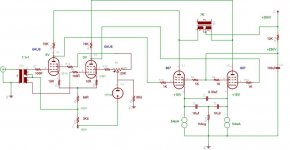
Heres what i came up with in the end.
All the values come amazingly close to the original Tabor amp design, so i think i'm in the right ball park. I still need to check over the math to make certain everything's OK.
i will try to run it by Gary Pimm, but I know he isn't keen on floods of enquires.
Shoog
All the values come amazingly close to the original Tabor amp design, so i think i'm in the right ball park. I still need to check over the math to make certain everything's OK.
i will try to run it by Gary Pimm, but I know he isn't keen on floods of enquires.
Shoog
Attachments
Neat cathode circuit for the 807's. 🙂
And bold use of DC coupling. I guess you could use coupling caps until you are confident that it works OK. With CCS on the output tubes you could probably also move the 807 grids up another 10-20 volts to have some extra margin for thermal drift and space for the CCS if required ?
The STC 807 app notes recommends a voltage divider for the 807 screens. Maybe something like 3.3/15K ?
- sorry I can't offer any advice on the original question.
SveinB.
Neat cathode circuit for the 807's.
Can't really take credit for it as it was Brian Becks idea originally.
And bold use of DC coupling. I guess you could use coupling caps until you are confident that it works OK. With CCS on the output tubes you could probably also move the 807 grids up another 10-20 volts to have some extra margin for thermal drift and space for the CCS if required ?
I was thinking the same thing about giving the CCS more breathing space. They should move the cathode voltage to keep everything stable over time. It should be a lot more stable than most direct coupled designs, only needing adjustment to the 6AU6 screens.
Shoog
So after weeks of building and months of planning, I finally got to the stage of commissioning this Tabor clone. I built very much as the above schematic. The only major change I made was to simply strap the screens of the 807 to the +B because Gary Pimm said this would minimise hum.
I did some staged testing - heater, VR150.
I finally got to the stage of trying to power it up for the first time. Oh dear sparks have flown and the silicone has gone to the great heaven in the sky. The problem is that the negative rail is silicone rectified and comes up about 15 seconds before the positive rail. This places a big potential across the CCS's just as they start to conduct. This exceeds their voltage rating and they go puff.
Good ideas often result in disaster hey ! So I have a problem, I could try rebuilding them but place zeners across them to clamp the voltage to a safe margin, though I think this will be hard on the zeners.
I could build a descrete CCS capable of taking 300V, but that will require ordering parts.
I could try the garter bias but that will take another 20 volts of bias.
I really want this to be self biasing with zero lifetime adjustment.
Any ideas.
One good thing that has happened is that the 6AU6's are conducting 5mA through the plate's - exactly as designed without any adjustment, though their plates are currently settling at about -18V rather than the planned 0V
Shoog
- Status
- Not open for further replies.
- Home
- Amplifiers
- Tubes / Valves
- Need some advice on a LTP input stage.