With some amplifier designs the vbe multiplier mounts with the driver transistors and not on the main heat sink.
You just want the maximum current to be well over what you want to protect from mistakes. Try to size the parts so the pot wiper is 1/2 to 3/4 travel at your "happy place". Single turn pots are best for this. These values should put you in range for component variables.
You just want the maximum current to be well over what you want to protect from mistakes. Try to size the parts so the pot wiper is 1/2 to 3/4 travel at your "happy place". Single turn pots are best for this. These values should put you in range for component variables.
Yup. I think it’s when you’re using Sziskai pairs you want to mate them with the drivers. Kind of makes sense, since the drivers determine the polarity of the pair.
Not sure what you mean by the current being well over what you want to protect from mistakes. I would make the current well below the point where things sizzle 😀
Not sure what you mean by the current being well over what you want to protect from mistakes. I would make the current well below the point where things sizzle 😀
Sorry, punctuation.
You want the current to be limited to prevent destruction from goofs, but enough range to be well over what you would want to allow for part variations.
Yes, I like Sziklai pairs in the output section, also good for signal sections. Diamond buffers have very high performance, but they are so fast they can oscillate if you aren't careful.

As one would like to have the effect of the current through the divider compared with Ic through the bias transistor as little as possible, whereas the effect of Ib is minor to the current through the divider, and knowing the relation Ic/Ib =β, the optimum value of 'Idivider' ("Id") would be:This is an example from an amp I designed a while ago. I think I would have made the resistor values lower if I did it again. You will have to adjust the resistor values to suit your design.
Ic > Id > Ib -> Id = √β * Ib = Ic / √β
With the BD139, say β = 100 and Ic = 10mA, Id = 1mA and Ib=0.1mA.
I want to offer comment about your bias scheme (which I like very much!), but first I want to ask about the closed-loop gain--- it seems unusually large.
Assuming I read Ref Des and the values correctly (print a bit fuzzy), gain is 1+(R09+R10)/R08 = 1+(27K+2.2K)/150 = 196 V/V, or about 46dB. Is this correct? Gain around 26dB would be more typical. Maybe R09 =2.7k ?
I think an input blocking cap would be a good addition; the amp's input resistance is 1M and any preamp blocking cap is likely to be several uF. Input settling time is likely several seconds.
C04 and C05 seem far too large and will be a follow-on topic.
Last edited:
Hi njswede,
I have attached the amended circuit based on the original schematic. Have also included some missing components that were not included earlier since a section was going to the overload protection. A portion of the original schematic is also included. Thank you
I have attached the amended circuit based on the original schematic. Have also included some missing components that were not included earlier since a section was going to the overload protection. A portion of the original schematic is also included. Thank you
Attachments
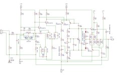
The VBE multiplier Q6 as per the schematic is mounted on the same heatsink as the output transistors.

I believe it will be extremely difficult to get it to work.
The circuit uses 6 capacitors c02,03,06,07,08,09 for phaze compensation to inhibit self oscillation.
With other transistors and layout some of them will have to be changed.
Difficult as they all depend on each other.
The circuit uses 6 capacitors c02,03,06,07,08,09 for phaze compensation to inhibit self oscillation.
With other transistors and layout some of them will have to be changed.
Difficult as they all depend on each other.
I am not getting the output transistor. However I am able to find onsemi MJ11032G NPN Darlington Transistor, 50 A 120 V HFE:400, 2-Pin TO-204 and its complementary pair onsemi MJ11033G. I know its not an equivalent but are these fast switching darlington transistors
Attachments
Those are NOT fast switching darlingtons. They are the double die version of MJ11015/6. That’s right, two parallel dies inside to make 50 amps. Their rated SOA is a little worse than two MJ11015 to account for imperfect current sharing. Their speed of course is the same as all old Motorola/ON old school darlington - no better (or worse) than TIP142/7.
I dont think it will work. You just can not replace 30MHz trnsistors with other of 8 or probably 4 MHz.
You will need to replace the 6 capacitors to higher values.
You will need to replace the 6 capacitors to higher values.
I don’t get the whole craze of trying to reproduce amplifiers with unobtainable components. I designed a Blameless inspired amp with the most bog standard components I could think of: 2N5551/5401, BD139/140 and IRFP(9)240 and it performs great. What is it you’re seeking with that design? If it’s the original sound, you’ve already changed it since you need to use different transistors.
- Home
- Amplifiers
- Solid State
- Need help with this audio amplifier. If this circuit can work?