Hello all. I have been having a devil of a time trying to get this circuit to work.
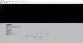
The upper CCS is supposed to be a power Jfet from united SIC with fixed bias working in class A and the lower device is supposed to be a CCS load.
The idea is to have the opamp bias the bottom device so that I do not have to use a bias resistor. By avoiding a bias resistor, the voltage drop across the CCS is minimized.
The issue with the circuit is that I keep getting 12.8v at the output instead of the intended 0v. I know I am doing something wrong/stupid, but I just can't seem to figure it out.
Any thoughts are appreciated.
Attachments
You may not have intended it like that, but your circuit is basically a CCS-loaded common drain amplifier.
Now name one important property of a common emitter / drain / cathode amplifier.
Hint: It's inverting.
This turns your negative feedback into positive feedback, hence the latchup.
You will have to either swap your inverting and noninverting input connections or mirror + rotate the opamp (F7, Ctrl-E, Ctrl-R) and F4 some V+ and V- labels to reconnect the upside-down power pins.
Also, R2 = 1000k is not likely to be a good value. Try R2 = 100 instead.
I'm not sure I completely get what you were trying to do. Did you want a CCS loaded unity gain buffer instead? Then your FET should have been at the top and the CCS on the bottom.
BTW, have you thought about the effect of FET parasitic capacitance at frequencies above DC in conjunction with finite gate current?
Awesome!!!! That got me 99% of the way there. I will put the pieces of my schematic back together and post back in a little while.
The idea is to have an upside down son of zen hybrid amp.
The idea is to have an upside down son of zen hybrid amp.
