Looking for help with JFET basics here.
I have J112, how do I calculate a basic common source circuit?
From simple research I found this: we care about two important parameters:
Idss - current that goes freely through the JFET (from Drain to Source) if there is no voltage applied to the Gate, called "zero-voltage gate current"
Vgs(off) - voltage applied between Gate and Source that will prevent JFET from conducting any current from its Drain to Source, called "gate-source cutoff voltage"

Looking at the J112 datasheet from onsemi we have two graphs. Why is there 0-40mA and 0-15mA scales?


For some reason it is considered a good practice to take Idss for a given JFET and use half of that. Why?
Assuming J112 Idss = 5mA, we are aiming at 2.5mA.
If dual power supplies are +-15V, we have drain resistor Rd = 15V/2.5mA = 6kOhm.
Looking at the graph we can match 2.5mA to Vgs around -0.3V.
Now, this is the part where I don't know how to continue to calculate source and gate resistors because it is dual supply.
Any help is much appreciated!
I have J112, how do I calculate a basic common source circuit?
From simple research I found this: we care about two important parameters:
Idss - current that goes freely through the JFET (from Drain to Source) if there is no voltage applied to the Gate, called "zero-voltage gate current"
Vgs(off) - voltage applied between Gate and Source that will prevent JFET from conducting any current from its Drain to Source, called "gate-source cutoff voltage"
Looking at the J112 datasheet from onsemi we have two graphs. Why is there 0-40mA and 0-15mA scales?
For some reason it is considered a good practice to take Idss for a given JFET and use half of that. Why?
Assuming J112 Idss = 5mA, we are aiming at 2.5mA.
If dual power supplies are +-15V, we have drain resistor Rd = 15V/2.5mA = 6kOhm.
Looking at the graph we can match 2.5mA to Vgs around -0.3V.
Now, this is the part where I don't know how to continue to calculate source and gate resistors because it is dual supply.
Any help is much appreciated!
Attachments
There are two scales because of the large exemplaric spread. Some units have in absolute value far greater pinch-off voltages and far greater drain currents at zero gate-source voltage than others. The transconductance at a given drain current doesn't vary all that much, though, as long as that current is below IDSS.
Do you have any requirements for your circuit?
Do you have any requirements for your circuit?
Gain of 2 probably. Or less
I am realizing that I might be better using voltage follower (common drain) schematics…
Still helpful to learn how to calculate either..
I am realizing that I might be better using voltage follower (common drain) schematics…
Still helpful to learn how to calculate either..

Gain of 2 probably. Or less
I am realizing that I might be better using voltage follower (common drain) schematics…
Still helpful to learn how to calculate either..
You want 2 V RMS into 1 kohm. Assuming sine waves (as done by default in audio), 2 V RMS is 2 sqrt(2) V peak, so the output has to be able to deliver 2 sqrt(2) mA peak to its load. The bias current therefore has to be at least 2 sqrt(2) mA and if forward gate-source biasing in the peaks is to be avoided, IDSS has to be at least twice that.
Assuming load means whatever is connected to the output, so excluding the resistor R3 that is used to bias the drain, you will need something extra because of the signal current through R3. Normally you don't want to go too close to zero momentary current to avoid excessive distortion. All in all, 4 mA drain bias current and IDSS >= 8 mA seem reasonable. That means only a part of the J112's will be suitable, as IDSS could be as low as 5 mA.
VGS is somewhere between -0.2 V and -2 V at 4 mA according to the plots you posted. Assuming a -15 V negative supply and a gate biased at 0 V, there will be 15.2 V to 17 V across the source resistor, average 16.1 V. The source bias resistor has to be about 4.025 kohm to get the desired 4 mA, so 3.9 kohm is the nearest E12 standard value.
To keep the JFET in saturation, the drain-gate voltage has to exceed -VGS,off. That means at least 5 V during the negative excursions of the output voltage, so at least 5 V + 2 sqrt(2) V in the bias point. Taking 8 V, which is already awfully close to 5 V + 2 sqrt(2) V, and assuming a positive supply of +15 V, the drain bias resistor R3 then has to have a value of (15 V - 8 V)/4 mA = 1.75 kohm, nearest standard value 1.8 kohm.
However, the 4 mA bias current is insufficient to supply 2 sqrt(2) V of peak signal voltage into 1 kohm in parallel with 1.75 kohm, so you either have to increase the supply voltage, or come up with some different method to bias the drain, or increase the bias current and go through the whole calculation again.
Assuming a +24 V positive supply, R3 = 3.9 kohm should do the trick.
To get a gain of -2, the transconductance then has to be 2 * (1/(1 kohm) + 1/(3.9 kohm)) ~= 2.5128 mS. The transconductance of the FET itself is about 12 mS at 4 mA according to the datasheet plots, so you need source degeneration. The resistor has to be 1/2.5128 mS - 1/12 mS ~= 314.6 ohm.
You get pretty close to that when you connect 330 ohm in series with a big (eletrolytic) capacitor (approximately 1/(2 pi fc (330 ohm + 1/12 mS)) ~= 77.01 uF for 5 Hz cut-off frequency -> 100 uF nearest E6 value) from the source to ground. The 330 ohm acts in parallel with the 3.9 kohm that biases the source, so together they are 304.3 ohm.
Don't forget to put a gate bias resistor of at least 47 kohm from the gate to ground, and a big capacitor from the drain to the load impedance to keep the DC current from flowing through the load.
Last edited:
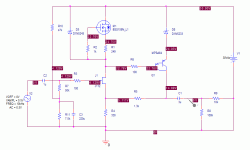
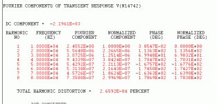
You may not like this as it uses feedback, but here is a design that has low distortion and low output impedance. Gain is X5, and you can adjust for different J112 characteristics by varying the input bias network.
Attachments

- Home
- Source & Line
- Analog Line Level
- Need help designing simple JFET J112 amplifier using dual voltage supplies