Hi!,
I constructed this Class AB amplifier called "S-Sub" which the author says it's designed specially for woofers. I want to use it in a biamped system. I recently made it but I cannot get it working, cause I have a problem with output DC.
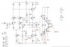
I have -25V at the output (obviously it's wrong), where the author says that this should be between -0,1V and 0,1V and then adjust it to 0V (or as close as possible) with the pot labelled R5b on the schematic.
Power supply used for the testing is +/-30VDC.
I have basics knowledgement on electronics and following the schematics I found that between D2 and R9 I should have -25,3V (-30VDC from the supply plus 4,7V from the regulating zener, it gives abaout -25,3V). I measured it with the tester and that's the value I got.
At that point we see it's linked to Q9 transistor's base, and I also have -25V at its collector.
The same value is measured at the base and emitter of Q13, base and emitter of Q14 and the base and emitter of the output transistor Q15...
I am missing lot's of things from the schematic because I don't understand it at all, so I couldn't diagnose where the problem is...
I atteched the schematic indicating the points where I measured with the tester.
I checked the circuit few times, found some others mistakes and corrected them, but now I don't know what I'm doing wrong.
Note: Transistors Q12, Q13 y Q14 are KSE350 (replacement for MJE350); and transistors Q6, Q7, y Q9 are KSE340 (replacement for MJE340) .
I also connected the circuit with two 22 ohm 5W series resistors (one at +V and the other at -V) for the testing...just in case...(I don't think they are causing this problem!)
Here is the link to the schematic:
http://www.pcpaudio.com/pcpfiles/proyectos_amplificadores/ampsub/etapa.pdf
Hope someone can help me!
I constructed this Class AB amplifier called "S-Sub" which the author says it's designed specially for woofers. I want to use it in a biamped system. I recently made it but I cannot get it working, cause I have a problem with output DC.
I have -25V at the output (obviously it's wrong), where the author says that this should be between -0,1V and 0,1V and then adjust it to 0V (or as close as possible) with the pot labelled R5b on the schematic.
Power supply used for the testing is +/-30VDC.
I have basics knowledgement on electronics and following the schematics I found that between D2 and R9 I should have -25,3V (-30VDC from the supply plus 4,7V from the regulating zener, it gives abaout -25,3V). I measured it with the tester and that's the value I got.
At that point we see it's linked to Q9 transistor's base, and I also have -25V at its collector.
The same value is measured at the base and emitter of Q13, base and emitter of Q14 and the base and emitter of the output transistor Q15...
I am missing lot's of things from the schematic because I don't understand it at all, so I couldn't diagnose where the problem is...
I atteched the schematic indicating the points where I measured with the tester.
I checked the circuit few times, found some others mistakes and corrected them, but now I don't know what I'm doing wrong.
Note: Transistors Q12, Q13 y Q14 are KSE350 (replacement for MJE350); and transistors Q6, Q7, y Q9 are KSE340 (replacement for MJE340) .
I also connected the circuit with two 22 ohm 5W series resistors (one at +V and the other at -V) for the testing...just in case...(I don't think they are causing this problem!)
Here is the link to the schematic:
http://www.pcpaudio.com/pcpfiles/proyectos_amplificadores/ampsub/etapa.pdf
Hope someone can help me!
Attachments
R17 does not look right to me. It would appear to defeat the working of Q9!
Q9 itself could be damaged. You may also need to adjust R6 for your use of an MJE350. I'd stick to BD139/140 unless you are able to work out and adjust part values appropriately. In addition, MJE340/350 are not good drivers (Q7, Q14) and may compromise performance.
What power transistors for the outputs are you using?
Do not connect a load to the output. This would very likely blow all your output devices.
Have you powered up through a light bulb tester?
Does the bulb stay lit?
more test voltages would help.
Vr3, Vr?, Vr4, Vr5, Vr6,
All the Zeners are dissipating very low Watts.
They will not regulate at all well if the Zener current<<10% of max rating.
Have you powered up through a light bulb tester?
Does the bulb stay lit?
more test voltages would help.
Vr3, Vr?, Vr4, Vr5, Vr6,
All the Zeners are dissipating very low Watts.
They will not regulate at all well if the Zener current<<10% of max rating.
To be honest, for a low power amp, it's not a fabulous design. For a subwoofer amp... I'm not impressed. How much power do you want in your sub?
I'm just going to suggest making sure that any transistor substitutes are in fact equivalent devices. And check that all transistors are installed with the correct lead orientation. Those are a couple of things that gave me trouble.
Just a wild guess - did you use 8R2 or 8K2 for R4? Correct would be 8R2 ( 8.2) More voltages would be helpful. Good luck.
hi! thank you all for the replies!
jaycee: at the author's web he says R17 is there to be "dominant" against other parassits resistances, also to reduce the high ("infinit") impedance and to not allow it (the impedance) to be variable...
I want this amplifier to be rated at about 100W at 8 ohm. So higher voltage is required, and the author suggest using MJE340 and MJE350 when using more than +/-40VAC (56VDC) because they support that higher voltage. He notifies that they are worse compared to BD139 and BD140...
I think the power supply would be something between +/-56V and +/-63V (this depends on the transformer I will be able to get), so I can get the decired power.
The output power transistor I'm using right now are MJ15024 and MJ15025.
I changed Q9 and Q12, now using BD139 and BD140 respectively, but still have the same problem...
Supposing that I switch back to MJE transistors, what value do you suggest for R6? (or explain me a bit, if you want, why should I change it and how to calculate it) 🙂
AndrewT: I haven't connected any load because of the high DC voltage at the output, I want to fix that first...
I didn't use a bulb, just 47ohm in series (for the first test) and now 22ohm (still testing...) and they don't get hot.
I will measure voltages across the resistors and zeners and post them in a few minutes!
dangus: I have already done that, anyway I will check everything again
sregor: That's a very good observation! R4 is 8.2 ohm. Unfortunatly I don't have a higher voltage supply right now
PD: sorry for my 'not very good' use of english!
To be honest, for a low power amp, it's not a fabulous design. For a subwoofer amp... I'm not impressed. How much power do you want in your sub?
It's not for a subwoofer but for an 8" woofer in a bi-amped system. As I said in the previous post I want about 100W @ 8 ohm (per channel)
Well, I didn't choose it because I wanted something special. The design is not complex, the author offers the PCB masks for free, I was sure I could get all the components needed, and I made the "Public" amp from the same author (which is the only DIY amp I have right now), and the author recommends it for the purpose I need... so at the time of making decisions I think there was no reason for not choosing it.
I consider I'm a beginner yet, so I didn't want to go for something more complex but very accurate (not for now!); I want to experiment a little more before!
I changed Q6 and Q9, they are now BD139. And BD140 for Q13 and Q12. I still have -25,3V at the output...
Measurements (using those new transistors):
VR3= 2,49V
VR?=0,23mV (yes, less than 1 mV)
VR4=0V (I put the tester at the 200mV scale and measured 0,00mV)
VR5=1,82V
VR6=1,72V
D1=4,13V
D2=2,41V (D1 and D2 are the 4,7V zeners)
D3=8,85V (it's the 9,1V zener)
(I measured voltage across each component, not taking GND or another point as reference)
Note: Input is shorted to GND
I think there is something wrong with D2 and have doubts about those 0V across R4...
VR3 = 2.49 and VR4 = 0 would indicate Q11 open. VR4 should be about 0.6 volts less than VR3. Also, since D2 has insufficient drop - would guess there may be a problem with Q5 or Q9 (base currents should be much less than the 2.5 mA going through R9. Also, by more voltages I only meant more voltage measurements, not higher voltages. Good luck.
Edit: Reread last post and saw you changed Q9. Maybe D2 is bad, but doesn't explain negative voltage at output.
Edit: Reread last post and saw you changed Q9. Maybe D2 is bad, but doesn't explain negative voltage at output.
Last edited:
I replaced the diode but nothing changed.
I removed Q5 (as I haven't got another one to replace right now), voltage across D2= 2,5V (aprox). I removed Q9 and measured 4,2V across D2.
Then I put Q5 back to its place, and measured again 4,2V across the diode. So Q5 seems not to be the problem...
When I put Q9 back to its place then I measured 2,5V😕. I removed R17 (considering what Jaycee said) and value measured was the same...
Also I replaced Q11 with a new BC559 but I still got 0,00V across R4...
I want to give it a try with BC639 (Q6) and BC640 (Q13), but I ran out of BC639s so I have to buy more... do you think it'll make any difference?
Reconsidered voltages. First, it seems as though Q9 is acting as a diode - nothing is pulling current through its collector - 25 volts across the R9 (10k) as about 2.5 milliamps, and 2.4v (Voltage drop across d2) - .6 (Vbe of Q 9) gives 1.8 volts across R6 (680) which is also about 2.5 milliamps. So that plus no voltage on R4 indicates most likely that no current is going through Q 11. With power removed, I would check continuity between R3 and base of Q 11, Emitter of Q 11 to R4, and the other end of R4 to the supply. Happy trouble shooting.
Hi guys, I have good news 🙂
As I had 0V at R4, checked the circuit, tested for continuity, everything seemed to be ok, I decided to test the BC559 transistors, (because I reached a point where things started to be senseless...)
I tryed measuring hFE with the tester but it was 0. I measured a new and unused BC559 and was also 0 (I could measure hFE with other transistors so the tester was ok)... so I thought (and according to what dangus said), what if the pins aren't ok? I checked for the datasheet and they seemed to be well mounted on the PCB (as I checked many times before), but what came as a surprise for me was that the BC559 hasn't "CBE" but "ECB" pin-distribution...
I inverted the transistor and crossed base and colector pins, connected power and measured VR4.. it was 3 (and something) volts... so things started to change. I could measure 4,2V at both zeners. I connected the tester to GND and the output and measured few mV😀.
Then I could easily adjust output DC with R5b preset.
I want to thank you all for your help! 🙂
I think it would have taken me years to find (or discover..!) that mistake.. (it never happened to me such a thing...).
Probably I would have abandoned the project!
Thank you so much again!!!
Tomorow I will test the amplifier whit a speaker and will tell you the results! (not now because it's 2:20 AM and I'm going to sleep!)
Cheers!
As I had 0V at R4, checked the circuit, tested for continuity, everything seemed to be ok, I decided to test the BC559 transistors, (because I reached a point where things started to be senseless...)
I tryed measuring hFE with the tester but it was 0. I measured a new and unused BC559 and was also 0 (I could measure hFE with other transistors so the tester was ok)... so I thought (and according to what dangus said), what if the pins aren't ok? I checked for the datasheet and they seemed to be well mounted on the PCB (as I checked many times before), but what came as a surprise for me was that the BC559 hasn't "CBE" but "ECB" pin-distribution...
I inverted the transistor and crossed base and colector pins, connected power and measured VR4.. it was 3 (and something) volts... so things started to change. I could measure 4,2V at both zeners. I connected the tester to GND and the output and measured few mV😀.
Then I could easily adjust output DC with R5b preset.
I want to thank you all for your help! 🙂
I think it would have taken me years to find (or discover..!) that mistake.. (it never happened to me such a thing...).
Probably I would have abandoned the project!
Thank you so much again!!!
Tomorow I will test the amplifier whit a speaker and will tell you the results! (not now because it's 2:20 AM
and I'm going to sleep!) Cheers!
Last edited:
R5b must be adjusted very close to minimal value so
the differential s current is high enough to allow enough
voltage drop through the resistor marked R? ( close to R3)
to make the VAS Q11 conduct and thus have the necessary
DC feedback loops setting the correct DC operating points.
Other than that , you can t use MJE 340/350 as Q7 and Q14 ,
as they are too low current devices to be able to drive
correctly the power devices.
All in all , as pointed by a member , not a very good implementation
of these kind of topology ,considering the whole schematic.
Hi , thanks for the replies
Considering your opinions about the schematic, next time I'll ask here for opinions BEFORE making a project jeje...
For the moment I'll test and use this amp for the woofer... but better amps may come in the future 😉
I have few questions about the transistors drivers, as many of you did not recomend to use MJE340 and MJE350.
I want to use +/-63VDC so I get about 110W power output @ 8 ohm. Should BD139/140 and BC639/640 support the desired voltage or it's too high for them?
(I think it's useful to remember that power transistors are MJ15024 and MJ15025... maybe I should change them). Also the author suggest changing R7 and R9 values to 33k when using more than 56VDC.
An alternative is to use +/-56VDC, maybe that way is safer, regarding the lower power output (which will be about 90W)
Those are final questions I have for this project
I'll wait for your comments 🙂
Cheers
mj15024/5 are excellent. Keep them............. many of you did not recomend to use MJE340 and MJE350.
I want to use +/-63VDC so I get about 110W power output @ 8 ohm.................................power transistors are MJ15024 and MJ15025...
+-50.5Vdc supply gives 110W into8r0 in my typical single pair output stage.
+-63Vdc supply should be capable of 200W into 8r0 if the system is designed properly.
MJE340/350 are slow, very slow. They have too low Ic max. They are designed for high voltage use, not audio drivers.
Since you are using MJ, try MJE15028/29 or 15030/31 or 15032/33 or 15034/35 as drivers.
.....
+-50.5Vdc supply gives 110W into8r0 in my typical single pair output stage.
+-63Vdc supply should be capable of 200W into 8r0 if the system is designed properly.........
In that case I would prefer 50VDC, because 200W would be higher than the rated power of the woofer (150W RMS)
......try MJE15028/29 or 15030/31 or 15032/33 or 15034/35 as drivers.
Thank for the recommendations!
Hello guys,
After few days I could finally get some time to buy the drivers components to replace for my amp, and all the others to build the second channel.
But I have some bad news.. =(
I replaced the transistor drivers, and when I was about to test the amplifier I had the same kind of problem again, not 24V but about 10 volts at the output.
For the moment I didn't take time to find the problem out because I wanted to build the second amp (and I thought it could be a silly mistake)
Once I finished it (the second amp), during the first test I measured again 24VDC at output (God has damned this amp!!😡) but this time voltage was positive, it seems that it's the same kind of problem but at the positive side. Voltage across D1 was much less than 4,7V... very similar case! so I thought the problem could be Q11 or Q12... replaced them and also replaced Qt but there was no luck...
Maybe I should leave this project , as I cannot find the problem out... now I have two stages that never worked🙁
I already made the crossover and it's voltage regulator so I won't give up, I want my woofer amp! (suggestions for 100W @ 8 ohm are welcome!!, and even better if I can use some of the electronics components I have!..)
If some of you guys want to help me giving it a final try, I did some measurements that may help:
VR1=0,104 V
VR2=0,419V
VR3=1,67V
VR?=1,88V
VR4=0,65V
VR5=21,67V
VR6=3,55V
VR7=11,37
VR9=23,56V
VR10=0,01 milli Volt
VR11= 0V
VR13=1,37V
VR14=1,372V
VR15=10,15V
VR16=0,011V
VR17=51,03V (it scared me...)
presets:
VR5b=9,51V (across extremes)
VRpolar=0,64V (across exremes)
D1 and D2 are the 4,7V Zeners:
V D1=1,44V
V D2=4,16V
D3 is 9,1 V zener:
V D3= 10,2 V
Thanks!
Edit: If any other measurement could be useful please let me know!
Last edited:
- Status
- Not open for further replies.
- Home
- Amplifiers
- Solid State
- Need help constructing amplifier S-Sub