Hi Munky,
you are not an idiot, you are just learning.
If you think that my implementation with 2 comparators will be too
complicated for you, you can use the method that Pafi is suggesting.
Use the resistor to charge the mosfet gate (turn-on) and the diode to discharge (turn-off). This will make the turn off much more faster that turn on introducing some dead time.
The amount of dead time is set by the resistor value.
Don't put capacitors on mosfet gates, you will only slow down something that is already too slow for 200KHz operation.
An IRF540 has around 2nF of gate capacitance, charge it trough the resistor and discharge it trough the diode. In this way the discharge time is set only by the maximum current that your gate
driver can sink (or source on the high-side).
Change your output filter and your load to 4ohm resistor
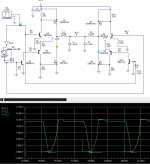
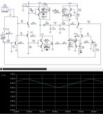
Hey, i have changed the load resistor back to four, and changed the lpf. Changing the lpf made a huge improvement, since there is barely any cross over. The signal response is still pretty slow, I tried to put the diodes into the circuit, but CircuitMaker keep running into errors. One problem is, when I put the pwm circuit with the hbridge circuit, nothing is working properly, I believe it is because the impedance doesn't match. What is the best way to do impedance matching? Thankyou for all the suggestions.
Attachments
Again:
I also don't know what do you want with these measurements. Where do you suppose to see the existence of dead time (or "cross-over")? And what do you measure actually? Y Axis is scaled in volts, and it seems to be real, but you have written I2_2 and I1_1 (currents) next to the curves.
Dead time is invisible with these measurements! Dead time means that Q1 have to switch off before Q2 switch on. You have to watch drain voltage of Q1 and gate voltage of Q2, or drain currents! Time relation between A and C is not really important!
With this value of R4,R9 (and R10,R13) Q2 (and Q7) never really turns on. They need -6 V of Vgs at least! (Now they get only 8V-12V=-4V)
But if you increased Vgs, they would cross conducted.
1st step: achieve fast gate charge and discharge. This needs high current (0,2 A minimum, but more is better). (You've got some ideas, take a pick!)
2nd: make charge a little slower, or delay it!
3rd: check if there is appropriate dead time! (Check drain currents and gate voltages too! This is why simulators are soo good: you can measure whatever you want!)
Note: discharging of a pMOS means making its potencial more positive, and vica versa.
This is a very interesting thread for me, but I wish I had found it a few months ago!
I'm working on a project for university designing a class-d amp on chip in a 0.35um cmos process, so its interesting to see how people are doing it with discrete components. Anyways, for my bridge, I changed the W/L of the drivers to change the rise/fall time. Rise/Fall time is equal to 0,69*Ron*CL, where Ron is your average on resistance and CL is your load capacitance.
I'm pretty sure these values would not need to be calculated in discrete components (since they are in the data sheets). I guess this isnt as relevant since you are using BJT drivers, but I thought I'd mention it anyways!
Hi Munky
Pafi is right, if you don't measure the drain current you can not
see if there is cross conduction or not.
I don't know why circuit maker is not able to measure the current on mosfet, but you can add a resistor in series of 0.000x ohm just to check the current (see attached schematics).
Your circuit is actually too slow for 200kHz and having a VGS on mosfets of only 4V means that their RDS_on is high and they are not fully switched on.
Change your driver structure to the one Pafi is suggesting in his link, or check the one attached, very similar to Pafi's one BTW.
For simulations (at least to see if there is some dead time) you can even remove the low pass filter. Check the current on the node connecting the P_mos drain to the N_mos drain. If there is no dead time you will see lots of current on that node.
Attachments
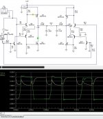
Hello, I've tried to implement the circuit for faster switching, so I used the totem pole and the diode idea. If I used something too close to pafi n maq's idea, I think my proff will kill me. I got a quick question though, when measuring the drain voltage, when the voltage is at -6V, does that mean that MOSFET is on? and what if it's pass -6V, is the MOSFET off at that point? Attached is the implemented circuit, do you fink the switching is ok? (Note: The dotted lines shows where -6V is at). THANKS
Attachments
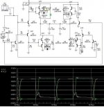
Hello, I've got rid of the LPF to see how much current goes through the drain of the MOSFETs. In the simulations it is giving me 3A of current, but when I had the LPF, the current dropped to like 0.5A for some odd reason. Attached is the current check coming out of the drain of the MOSFETs without the LPF.
Attachments
I've got rid of the LPF to see how much current goes through the drain of the MOSFETs
On that resistor you can see the difference (or sum, depending on reference directions) of the two (high and low side) drains! Kirchhoff's first law! You should measure current directly in the drains (or source, not a big difference).
You should make basic knowledge clear first! And practice on more simpler (ideal) circuits.
The current drops alot, is it because of the inductor?
Yes, this is it's job! On high freq it have to block the current, since it is useless, unwanted on output! It has to pass through only audio freq!
I got a quick question though, when measuring the drain voltage, when the voltage is at -6V, does that mean that MOSFET is on?
I hope you ment gate voltage (more precisely Vgs)! Yes, Vgs=-6V means on state. So you have a huge cross conduction. Q2 is already on at t=55.1 us, but Vds is very big on it, so there must be a very high current on it. Between t=55,1 and 55,3 us Vds is about -10 V, Vgs is 8...10 V. See attachment! This current flows through Q1, but of course doesn't go out to the load.
Now you are before the 2nd step!
Attachments
Hi Munky
When I was telling you to remove the filter I mean to remove the filter and the load. So the upper P-mos connected ONLY with the lower N-mos without anything between the two sides of the bridge.
Your 0.000x ohm resistor will actually measure the total current flowing by cross condution + the current flowing into the load + the current flowing into the filter capacitor.
Remove the filter AND the load, so that there will be no connection between the two sides of the bridge and then measure the current flowing trough the mosfets (thanks to the 0.000x ohm resistor) and the gate voltage (voltage between GATE and SOURCE).
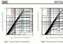
Any mos device will start to conduct current when its voltage between gate and source is greater than the treshold voltage (Vth). Check for Vth on the irf540 and irf9540 datasheet and you will find which voltage is allowed to avoid cross conduction (or better use the curves that Pafi is showing you on datasheet).
BTW: what is the value of your gate resistor? (the one in parallel with the diode), I can not read it from your schematics.
Use something bigger than the 2N3904 for driving the gates, it is rated only 200mA, maximum. The BC637 or something similar will do the job
ciao
When I was telling you to remove the filter I mean to remove the filter and the load. So the upper P-mos connected ONLY with the lower N-mos without anything between the two sides of the bridge.
Your 0.000x ohm resistor will actually measure the total current flowing by cross condution + the current flowing into the load + the current flowing into the filter capacitor.
Remove the filter AND the load, so that there will be no connection between the two sides of the bridge and then measure the current flowing trough the mosfets (thanks to the 0.000x ohm resistor) and the gate voltage (voltage between GATE and SOURCE).
Any mos device will start to conduct current when its voltage between gate and source is greater than the treshold voltage (Vth). Check for Vth on the irf540 and irf9540 datasheet and you will find which voltage is allowed to avoid cross conduction (or better use the curves that Pafi is showing you on datasheet).
BTW: what is the value of your gate resistor? (the one in parallel with the diode), I can not read it from your schematics.
Use something bigger than the 2N3904 for driving the gates, it is rated only 200mA, maximum. The BC637 or something similar will do the job
ciao
Hello,
I've tried to check for currents in CircuitMaker and for some odd reason I can not check the drain current. Also, in the simulations, there is no gate current, which doesn't make any sense. The source current seems ok. Attached is the simulation to check current. Also, should I decrease the gate voltage? do you think the current is too high coming out of the MOSFET?
I've tried to check for currents in CircuitMaker and for some odd reason I can not check the drain current. Also, in the simulations, there is no gate current, which doesn't make any sense. The source current seems ok. Attached is the simulation to check current. Also, should I decrease the gate voltage? do you think the current is too high coming out of the MOSFET?
Attachments
do you think the current is too high coming out of the MOSFET?
Yes, of course! This is 100 W idle loss approximately. There should be less then 2 W!
Also, in the simulations, there is no gate current,
There is, but only 1 pixel at this scale. Change Y axis!
And actually you haven't measured gate current. You've measured current of gate resistor. Gate current is sum of current of gate resistor, and current of gate-diode! Kirchoff's first law again!
the resistor parallel to the diode is 10ohms
Increase it!
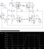
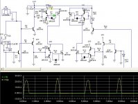
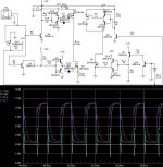
Hello, I'm still kind of stuck on making the fall time faster, I've tried the totem pole and the diode, and I don't think it's working as planned. Attached is the graph for the current of the source, as you can see, both MOSFETs on at the same time. Any suggestions please.. THANKS
Attachments
Hey Munky, of course you have cross conduction, you are
driving the high side and the low side out of phase....
This means that when the N-MOS is on the P-mos is on too, this explains your 40A trough the mosfet sources.
Remove transistor Q9 and related compoents and drive the
N-mos exacly like the P-mos. Q9 is an inverter that reverse the phase of the gate voltage applied to the n-mos.
_To make a quick try remove the LPF and the load
_ remove Q9 and related components
_ check for gate voltages and drain current on the mosfets
_ adjust the gate resistor to increase the dead time
ciao
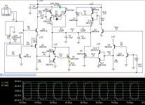
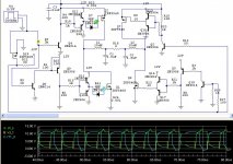
Hey, if I get rid of Q9, that will make both drivers driving the same thing. Without Q9, there will be 2 low side drivers. I thought I was suppose to get the currents to be out of phase, so the MOSFETS will not be on at the same time. Attached is the circuit without Q9, top 2 signals is the voltage of the gates and the bottom 2 signals is the current of the drain.
Attachments
Hey Munky,
now you are closer to make it work but there is still cross conduction.
Ideally with your current simulation setup you will see no current across the mosfet. You still have spikes of 2.5A (yellow and green trace). This means that during that time the P-mos is on also when the N-mos is on.
Adjust the value of the gate resistors (increase it) and check the current trough the mosfet.
No! you have a P-mos and an N-mos, the P-mos conducts when its VGS is negative, the N-mos conducts when the VGS is positive.
If you drive them out of phase you will always have both conducting at the same time by design.
now you are closer to make it work but there is still cross conduction.
Ideally with your current simulation setup you will see no current across the mosfet. You still have spikes of 2.5A (yellow and green trace). This means that during that time the P-mos is on also when the N-mos is on.
Adjust the value of the gate resistors (increase it) and check the current trough the mosfet.
I thought I was suppose to get the currents to be out of phase
No! you have a P-mos and an N-mos, the P-mos conducts when its VGS is negative, the N-mos conducts when the VGS is positive.
If you drive them out of phase you will always have both conducting at the same time by design.
- Status
- Not open for further replies.
- Home
- Amplifiers
- Class D
- Need Help: Class D Cross Over