Greetings!
I would like to as for your assistance in identifying a semiconductor. It is from a ROAD 220 bass guitar amplifier, power amp stage. The part was mounted on the driver pair heatsink and, in circuit, is wired across the PNP/NPN driver compliment from base to base. I'm really stumped because of the odd ID, and odd case style. I'm sure it is part of the thermal regulation of the output bias. I'm unsure if it is either a transistor or a diode array.
Google has not turned up either a schematic for the amp or anything that matches the markings on the part. One leg of the item was completely blow off. The drivers and output transistors were all shorted C-E.
Thank you for your help,
Gary
An externally hosted image should be here but it was not working when we last tested it.
it looks
like early bjt ....just right after change from germanium to piritioum bjt ....it looks like midle power like the bd 139-140 ....since schematic is not available ( i looked for my shelf also with no results )
there is only few things you can do
A) ...make a private mail to carlos destoryer x panzertoo@yahoo.com he is older guy may be he knows or remeber something more
B) make of small schematic of componets involved ...meaning that if this is in the driver stage and you also know the output devices then from location will understand if its a p- or- n and then given the power and rail voltage you will be able to replace both drivers !!!!!! with a complementary pair like bd 139-140 or mje 340-350 .... but then of course you have to re idle and ofset the amp and perform all related tests about performance and stability
C) if this is in the bias stage then from circuit you will be able to determine if its a p -or-n device and then again you can replace it with any of the above but still you have to re-idle ,offset, and perform test on the amplifier ......
keep in mind that most of the electrolytics of an old device are probably so good as a deep fried swordfish ha ha ha ha ....
meaning that all of them should be replaced any way .....
these are my advices but i am also gona keep looking for a schematic
From memory the Bass 220 head was one of the former of Rickenbacker amplifiers - that were using a conventional power amplifier circuit: LTP and VAS with CCSs (shared reference formed by two silicon diodes), BJT based Vbe multiplier and CFP output (fast MPSU drivers and TIP... outputs).
Vbe multiplier had a TO-92 cased 2N5088 transistor as thermal sensor, mounted on the drivers common heatsink.
Your picture shows something from the solidstate stoneage in an early TO-126 style case.
Draw back the schematic of the power amplifier from the PCB, if it's like I described (conventional CFP amplifier) then try something industrial standard NPN BJT as replacement, say a BD139. Don't forget to mount that on the drivers common heatsink, and of course, use thermal compound.
Good luck on your repair.
Anyway a high-resolution photo taken of the power amplifier stage's PCB would help.
Road Electronics was founded by Bud Ross; the same guy who also founded Kustom (Ross Inc.) and Ross Systems. The company was later sold to West L.A. Music that sold it to Rickenbacker that sold it to Celestion. Rickenbacker even introduced a Road series of amplifiers but I have an impression these were “bargain bin” quality compared to Road amplifiers introduced before the Rickenbacker era. The way I see it, you could inquire circuit diagrams from some places (namely from Rickenbacker) but there’s a good chance that “no-one” really has them. You won’t find the schematics from some Internet site (at least for free) – that I can pretty much guarantee. I would follow Sakis’ advice and sketch out the required parts following the circuit board layout.
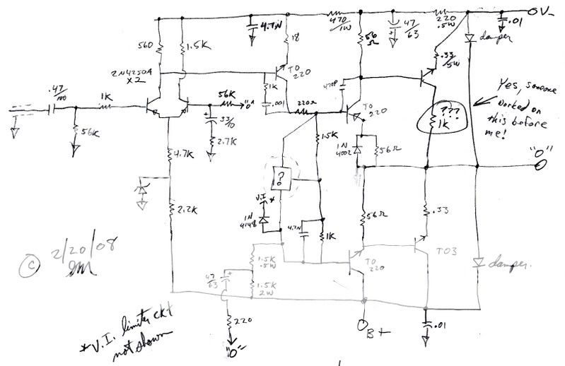
Thank you all for the replies and suggestions! I searched Schematic heaven but there was nothing. I'm sure the device is a transistor but the pinout and polarity has me baffled. The poweramp PCB has a quasi-complementary input circuit. The front end differential pair are PNP semis with an emitter current source circuit, driving a single NPN To220 device that is class A. Next, the drivers are Complimentary PNP/NPN T0220 devices, driving the two NPN outputs, which are NPN's. The amp has direct coupled output and a split +/- supply.
Okay, so the drivers have two 1K ohm resistors wired between the bases in a voltage divider. Two legs of my unknown device go to the driver bases with the third going to the center of said resistor divider.
Do the markings on the device look familiar to anyone?
Best regards,
Gary
Okay, so the drivers have two 1K ohm resistors wired between the bases in a voltage divider. Two legs of my unknown device go to the driver bases with the third going to the center of said resistor divider.
Do the markings on the device look familiar to anyone?
Best regards,
Gary
it seems
that this device then is related to the bias circuit ..... for shure a schematic or a foto would much better explanation .......
some procedures
most comercial amps regarding bias area have this transistor and a network of diodes or resistors with a trimmer to ajust idle ..... the transistor is located on the heatsink for thermal compensation IE when amp gets warmer bias goes down for safety reasons.....
some amplifiers do not include a trimmer and bias is
"""" about"""" fixed with a standard resistor meaning ...that for the particular amplifier a bit less or more bias will not make a serious difference ..... so not realy importand for bias to be ajusted ....
conclusion ....
if you just simply replace the transistor with any of the sugested and presuming that your amplifier does not come with a trimmer to ajust the bias ......
you will have to use a variac for starts and monitor bias and idle as voltage increases ..... if idle its mooving to margin of 50-100ma then you proceed ..... and after come to the full operating voltage you load the amlifier to specified output power to notice any thermal increase or instability .....
if not working correct trimmer needs to be added to match your new device to the circuit since the transistor you choose may work but far away from specs ....
A) thats why schematic is needed
B) ALL THESE APPLY GIVEN AS A FACT THAT THE REST OF COMPONETS ARE STILL WORKING AT YOUR AMP DIODES OUTPUTS DRIVERS ELECTROLYTICS ......
i feel like creating a service manual on line ha ha ha ha ha .....
best of luck my friend
Okay, so the drivers have two 1K ohm resistors wired between the bases in a voltage divider. Two legs of my unknown device go to the driver bases with the third going to the center of said resistor divider.
Any trimmpot there?
It just looks like an early TO-126 style device to me, being used as a VBE multiplier.
I'd take a gamble and substitute a BD139 or an MJE340 in there. I'd add a trimpot though, where the 1K resistor between it's base and collector would be.
It looks like a pretty conventional quasi complementary output amplifier otherwise. The diode leading off to "VI" looks suspicious - maybe this is what fried the VBE device in the first place.
What are the rail voltages?
Thanks Jaycee. That diode is part of the V.I. Limiter circuit which I did not complete in the drawing. The rail voltages are in the +/- 36 to 40 volt range. I haven't fired it up yet so the voltage is just a guess.
With a simple BJT like BD139 the bias voltage would be only 1V (0.6V×[(1.5k+1k)/1.5k]).
Your circuit needs about 2.4V for class B output bias.
I'd replace the 1.5k resistor in the Vbe-multiplier circuit with a 220...270 Ohm resistor in series with an 500 Ohm (470 Ohm) timmpot, then I'd adjust 20mA bias current in the output (6...7mV on the 0.33 Ohm resistors).
Your circuit needs about 2.4V for class B output bias.
I'd replace the 1.5k resistor in the Vbe-multiplier circuit with a 220...270 Ohm resistor in series with an 500 Ohm (470 Ohm) timmpot, then I'd adjust 20mA bias current in the output (6...7mV on the 0.33 Ohm resistors).
The part was mounted on the driver pair heatsink and, in circuit, is wired across the PNP/NPN driver compliment from base to base.
Strange. In a such quasi-complementary, non-CFP amplifier circuit the thermal sensing element need to mounted on the output devices main heatsink.
- Status
- Not open for further replies.
- Home
- Amplifiers
- Solid State
- Need amp repair help - Can you ID this semiconductor?