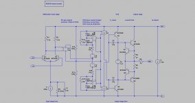
hello, attached you will find three different NE5534 models to be used with LTspiceIV. The _h1 model tries to be the most accurate with the differential input pair non-linearities, VAS slew-rate limitation, output stage non-linearities and output current limitation. The _h2 model is a simplification exhibiting a very wide bandwith, no slew-rate limitation and less THD than a real NE5534. The _h3 model is a near-ideal opamp introducing the smallest THD. See attached .zip. Those three models are compatible with the Kuroda topology and the Floating Supply Bridge topology. The behaviour of the supply pins is exact. Internally, the three models don't use any grounded reference.
Once you understand the method, you can adapt the models to other opamps.
Use more bias current in the VAS, increase the DC gain, decrease the compensation capacitor, ...
Replacing the BJT differential input stage by a NFET or a PFET differential input stage in the _h1 model is also possible, for simulating FET audio opamps.
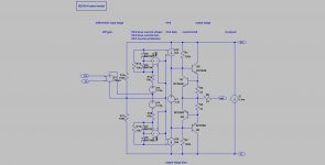
Attachments

Thanks, this is very interesting. Do you have a procedure for calculating the components values to match the op. amp. specifications ?
It should, provided the voltage controlled sources are present in the LTSpiceIII librairy. There is nothing special, no magic. And the models don't use any arbitrary sources. You are coming with an interesting question. Why would you prefear running LTSpiceIII when LTSpiceIV is freelly available here Linear Technology - Design Simulation and Device Models ?Thanks - will these (in particular the H1 model) work with LTSpice III also?
First step is to download the datasheet of the opamp to be simulated.Thanks, this is very interesting. Do you have a procedure for calculating the components values to match the op. amp. specifications ?
Second step is to determine the kind of differential input stage. This is explicit with oldschool opamps like the NE5534 (NPN pair), TL071 (PFET pair) and OPA134 (PFET pair). You get the info through a simplified schematic showing in the datasheet or by searching "FET" in the datasheet text. More tricky are the newest rail-to-rail input opamps where you may have two nested input stages. As an option, you may use custom-defined transistors in the input stage for better coping with the input bias current (BJT cases) or with the input transconductance (FET cases). Unfortunately, from the datasheets we don't know what are the collector (or drain) currents in the input pair, and we don't know the values of their collector (or drain) loads. I guess that a decent value could be 200µA each and 3K3 in then context of a general-purpose audio opamp. As an option, you may add a tiny voltage source as input voltage offset.
Third step is try to mimic the slewrate documented by the datasheet. A good starting point is to define the VAS bias current equal to 200µA, combined to a 10pF compensation capacitor. A faster opamp may operate at 500µA and/or 5 pF. A slower opamp may operate at 100µA and/or 20 pF. Tune the VAS bias current and compensation capacitor using the slew-rate application schematic. I have not tried simulating pathological opamp having asymetric slewrates like 3V/µs positive and 10V/µs negative. In order to do so you may try replacing one branch with a constant current source (or sink), with only one NPN as VAS and associated compensation capacitor.
If the datasheet specifies a 50V/µs slewrate or more, consider the _h1 schematic as not appropriated. In such case you'll need to use another topology documented as "non slewing" or "current feedback" or "diamond".
Fourth step is to try to mimic the DC open loop gain documented by the datasheet. The former steps may have eaten all remaining design freedom. This is why I've introduced a dedicated voltage gain block using a controlled voltage source between the differential stage and the VAS. Tune this gain block gain using the open-loop application schematic. I have no better solution.
Fifth step is to try to mimic the output stage fidelity (quiescent current related), current limit, physical resistors in the current limit section, and physical resitor in series with the output pin. If you read the TL071 datasheet, you'll know all resistor values. For other opamps you'll need to guess. General purpose audio opamps like the TL071 may use a small quiescent current in the emitter followers, something like 1mA or less. I'm guessing that a NE5534 may use a greater quiescent current in the emitters followers, something like 2.5mA maybe. Use the voltage source for setting the AB quiescent current. You may simulate pathologic opamps exhibiting an asymetric sink and source current capability using a BC546B NPN transistor, and a custom-made weak PNP transistor exhibiting less current gain and more parasitic capacitance. You may also replace all PNP transistors by custom-made weak PNP transistors, eventually compounding them with a NPN for emulating a strong & slow PNP functionality. This way you can better emulate the output sink and source characteristics, along with the dropout voltages. Where a rail-to-rail output characteristic matters like in the newest T.I. audio opamps, you may modify the output stage, replacing the emitter followers by CFP compounds.
A nice investigation path would be to analyse the class AB behaviour of the output stages using a dedicated test gear, graphing the power supply pin current. This is something you cannot get from the datasheet. Using such test gear, you may determine if the opamp is using a plain class AB output stage with one of the two transistors going off under heavy load, or using someting more elaborate like a soft non-switching class AB scheme.
Sixth step is to see what's the total current taken by the opamp, and compare it to the datasheet figure. Use a plain current source between +VCC and -VCC to adjust the total current. Add a resistor in parallel if you want more precision, like emulating the supply current increase with the supply voltage.
Seventh step is to deal with the negative power supply, positive power supply and common mode rejections. At DC and in function of the frequency. The resistor and capacitor in parallel with the current source biasing the long tailed pair is a first attempt. I still need to make a dedicated application schematic for doing the fine tuning.
Regards,
Steph
Last edited:
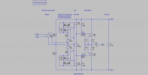
First step is to download the datasheet of the opamp to be simulated.
....
Regards,
Steph
This a great explanation, thanks. However, I hope I won't ever have to go through all that, that is the manufacturer models will be sufficient for my purposes.😛
Yes, you are right. You won't need the above opamp models if you don't deal with the Kuroda topology and the Floating Supply Bridge topology. Best regards.This a great explanation, thanks. However, I hope I won't ever have to go through all that, that is the manufacturer models will be sufficient for my purposes.😛
- Home
- Amplifiers
- Chip Amps
- NE5534 LTspiceIV models