Hi,
I planning to make a new prosject and I just want to confirm the impedance and construction of the converter from unbalanced to balanced audio.
I will connect this preamp i building to a Dynamic Presicion amp. 🙂
I have 3.96 volt with 2k in impedance from the tda7439 sound processor,
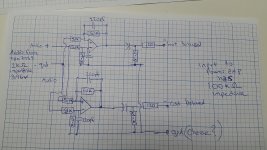
I attach the scematics i planning to build.
I would like som advice or corrections. please 🙂
best regards Niklas.
I planning to make a new prosject and I just want to confirm the impedance and construction of the converter from unbalanced to balanced audio.
I will connect this preamp i building to a Dynamic Presicion amp. 🙂
I have 3.96 volt with 2k in impedance from the tda7439 sound processor,
I attach the scematics i planning to build.
I would like som advice or corrections. please 🙂
best regards Niklas.
Attachments
I constructed and tested a similar circuit.
You need a buffer in the input path.
But: the circuit will oscillate.
You need a buffer in the input path.
But: the circuit will oscillate.
Check your two feedback circuits.
Compare to an "instrumentation amplifier", which uses 3 ICs.
And read Putzeys' G word article.
Compare to an "instrumentation amplifier", which uses 3 ICs.
And read Putzeys' G word article.
Your circuit will work (apart from the missing buffer and the oscillation).
You should better use a driver from TI/BB: DRV134PA.
You should better use a driver from TI/BB: DRV134PA.
Hi,
I planning to make a new prosject and I just want to confirm the impedance and construction of the converter from unbalanced to balanced audio.
I will connect this preamp i building to a Dynamic Presicion amp. 🙂
I have 3.96 volt with 2k in impedance from the tda7439 sound processor,
I attach the scematics i planning to build.
I would like som advice or corrections. please 🙂
best regards Niklas.
Take a look at these: View attachment The G Word Copy.pdf and View attachment gain_appnote Copy.pdf
Mike
Hi,
The channels are identical, it doesn't do balanced.
rgds, sreten.
True but Sony has built thousands of machines with this same mistake. It's not worth the time to correct them.
G²
I have not analyzed the circuit in detail, but you need at least two things:
1. Swap the + and - inputs of the op-amps. As it is now there is positive feedback.
2. You need some kind of ground connection as well to avoid a potentially large common mode signal.
1. Swap the + and - inputs of the op-amps. As it is now there is positive feedback.
2. You need some kind of ground connection as well to avoid a potentially large common mode signal.
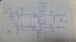
remake
here, i added buffer, changed the second stage to positive feedback,
and i guess it has a ground connection throug the sheild connected to the chassie(or the pcb cards on each side.)
i got a lot of different views and replies i
i would admit that i get a little confused....
best regards and thanks for replies.
Attachments
I guess you should check the datasheet of the BB/DRV 134PA.
http://www.ti.com/lit/ds/symlink/drv134.pdf
http://www.ti.com/lit/ds/symlink/drv134.pdf
See also the SSM2142 and THAT 1606/1646. Both the DRV134 and SSM2142 rely on precision resistor trimming to control positive feedback, as do similar circuits implemented with off-die resistors, so I would not recommend attempting to implement these topologies with NE5532s without greater understanding. At minimum I'd suggest learning to do simulations as these will catch errors many errors much more subtle than the current confusion over which terminal to use for feedback.
You may find figure 3 of the LME49724 datasheet also of interest.
You may find figure 3 of the LME49724 datasheet also of interest.
You still have the wrong polarity on the inputs of the two output op-amps. Apart from that, I think it will work, provided you have the shield or something else to connect the GND of this circuit and the GND of the source equipment (TDA7439).
The buffer for the GND signal may not be needed, since the GND will hopefully have a very low impedance.
The buffer for the GND signal may not be needed, since the GND will hopefully have a very low impedance.

See Self's "Small Signal Audio Design", 2nd edition p355, fig 19.8a.
The circuit has a unity gain op-amp stage to buffer the input signal.
Its output provides the hot output of the balanced stage.
It also drives an inverting op-amp stage, gain -1 set by two 1 kOhm resistors, the second (feedback) one being in parallel with a 100 pF cap. The output of this second op-amp provides the cold output.
Both op-amp outputs have a DC decoupling cap and a 68 Ohm resistor in series connected to an XLR connection (hot pin 2, cold pin 3).
The dual op-amp is the NE5532.
This circuit is intended to be loaded only by a differential stage.
The number of components and the price are very low, the performances are very high.
Jens h. I missunderstood. Thoght it would be a positive feedback. But you meant There shoukd be a negative feedback. ?
This willl not work correctly.
- Status
- Not open for further replies.
- Home
- Source & Line
- Digital Line Level
- ne5532 for balanced xlr