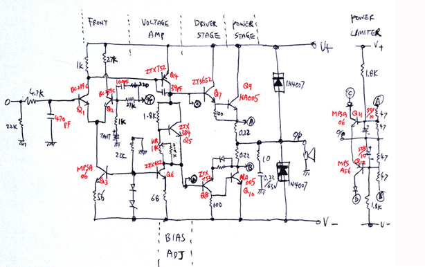
How would that work?The 27R collector resistor in the NAP250 design, I believe, is used to fine-tune the tempco of the bias generator.
The voltage across the collector resistor is basically set by the current source (or sink) for the VAS. It is thus constant with temperature. It is subtracted from the output of the Vbe multiplier.
So to get a given bias voltage you need a higher multiplication factor in the Vbe circuit to counteract the voltage lost across the collector resistor
Thus the tempco is increased as the collector resistor value is increased, since the multiplication factor has to be increased. This allows for over-compensation.
The collector resistor can also correct for supply rail variation if the current source isn't perfect, so that the bias doesn't change when the mains voltage is verying. Increased current would increase the Vbe multiplier's Vbe, but also adds to the voltage dropped in the collector resistor - you can arrange that these approximately cancel.
It can't do both of these things perfectly (unless you are lucky)...
Last edited:
Thanks for that Mark, I didn't fancy searching for articles on the topic as it's not often raised. Self includes an explanation in his Class A/B/AB or whatever you like trimodal amplifier discussion.
Oh I see where you are both coming from now.
First, Douglas Self is not an audiophile capable designer. His paint-by-numbers approach is never going to give birth to a Michelangelo. Be careful who you learn from.
This "Trimodal" design uses a Vbe multiplier in a different configuration to Naim's. So the temperature effects you mention do not apply to the Naim. Besides that, I thought the Self idea was to set the collector resistor to minimize changes in Vce with current.
Attachments
Love the analogy yes Self is very much a paint by no's Having said that I have enjoyed all his books and for a paint by no's guy follow his advice and you will get a decent working unit . But stretching a point his amplifiers have and i have to be careful with this comment
have no soul or real originality Yes his work is analytical and to an extent accurate but for me implementation is is as important as design
Trev
have no soul or real originality Yes his work is analytical and to an extent accurate but for me implementation is is as important as design
Trev
Agreed, though I wouldn't assume that anything written by a non-audiophile must be suspect or design elements they discuss shouldn't be in your amplifier lest they impinge on sound qualities. The NAP circuit was designed, adapted and applied by others before being adopted by JV, and long before Self's articles and texts were published, after all.
Regarding the Trimodal design, I was recalling discussion in (and I can't locate mine) the 3rd edition 1997? As shown, the latest, 6th edition doesn't appear to discuss the same design and details - sorry to mislead. However, there's a separate chapter on thermal compensation in most editions. In the current 6th it certainly is, including details of the collector resistor's role and selection, beginning at Variable-tempco Bias Generators ch 22, p530.
Regarding the Trimodal design, I was recalling discussion in (and I can't locate mine) the 3rd edition 1997? As shown, the latest, 6th edition doesn't appear to discuss the same design and details - sorry to mislead. However, there's a separate chapter on thermal compensation in most editions. In the current 6th it certainly is, including details of the collector resistor's role and selection, beginning at Variable-tempco Bias Generators ch 22, p530.
No one should pay £50 for his book.
Ian, can you paraphrase this temp compensation thing? Or maybe don’t bother unless you think it applies to Naim designs.
Ian, can you paraphrase this temp compensation thing? Or maybe don’t bother unless you think it applies to Naim designs.
I think Mark has already done that adequately, as it applies to Naim (NAP) designs, at least the models I recall. Its a conventional arrangement and about the simplest way to set the tempco to track a particular output and thermal coupling to the output stage. However, like some other refinements, it wasn't used in NAP90 or any early Nait models, as I recall.
I suggest downloading a PDF of an old version of the handbook, like the 4th edition reading from p372. The text is a little shorter but it contains similar circuits and explanations which compare well with those of either the standard NAP250 schematic or Avondale's yellow NCC200 variant which are everywhere on the 'net. It's a lot less than £50 (virtually free), takes a minute or so and has been available for some years.
Audio Power Amplifier Design Handbook, Fourth Edition - PDF Free Download
Member
Joined 2009
Paid Member
Idea - maybe try using spice on that Vbe design - I have found spice simulations very helpful for testing out the thermal feedback loop and that's primarily why I chose the design approach I did for my clone (TGM10).
I've found Self's writings to be one of the more useful in my early learning in this hobby, the various topics bring a clear engineering approach that underpins good audiophile design as well as introducing some key concepts, acronyms and some debunking.
Price of specialized books has always been outrageous. I find most of the material I want on the internet - much of the key stuff has been published (legally).
It's a pity that JV didn't publish - we're all guessing what he intended, few folk had the opportunity to get information from the source.
Last edited:
The problem with spice there, is how to model the air transfer of heat in a Naim quasi design, as the response time lag is so very long. I guess you can calibrate the model by practical tests but that's a level of difficulty I'd avoid, if possible.
If my memory serves me correctly, I think you reworked the design and wound up with a a more normal, fast response from the Vbe multiplier in TGM10.
If my memory serves me correctly, I think you reworked the design and wound up with a a more normal, fast response from the Vbe multiplier in TGM10.
Member
Joined 2009
Paid Member
Yes my design was different and avoided the delay through the air. But I wasn’t suggesting you simulate that but rather you simulate the thermal extra resistor in the collector of the multiplier and see if it produces the behaviour described previously Even assuming direct thermal contact with the output you can vary the resistor and see if it provides control over the thermal feedback
This does not apply to the Naim circuit. The driver bias voltage is taken across the whole Vbe multiplier. Changing the collector resistor does not require adjustment; only the Vce is changed.The voltage across the collector resistor is basically set by the current source (or sink) for the VAS. It is thus constant with temperature. It is subtracted from the output of the Vbe multiplier.
So to get a given bias voltage you need a higher multiplication factor in the Vbe circuit to counteract the voltage lost across the collector resistor
Thus the tempco is increased as the collector resistor value is increased, since the multiplication factor has to be increased. This allows for over-compensation.
The collector resistor can also correct for supply rail variation if the current source isn't perfect, so that the bias doesn't change when the mains voltage is verying. Increased current would increase the Vbe multiplier's Vbe, but also adds to the voltage dropped in the collector resistor - you can arrange that these approximately cancel.
It can't do both of these things perfectly (unless you are lucky)...
Attachments
Last edited:
Thanks for the link.I suggest downloading a PDF of an old version of the handbook, like the 4th edition reading from p372.
Audio Power Amplifier Design Handbook, Fourth Edition - PDF Free Download
Chapter 1 summarizes Self's approach to audio research.
Attachments

Member
Joined 2009
Paid Member
Just want to point out that the reason you don't find integrated CFPs is that real NPN and PNP transistors are made on different types of silicon, N or P type. When you integrate more than one transistor, you have to pick one or the other type of silicon, so you get poor PNPs on a N type chip and poor NPNs on a P type chip. Discrete PNP transistors do suffer some issues, but not like integrating both types.
Also, there is no good way to cross couple CFPs. Cross coupling is a big improvement in cross-over distortion, speed, and thermal stability. Now that we have 40MHz power transistors, it's perhaps not as important, but older BJT failures were often due to shoot-through current when driven above ~10KHz, because a passive pull-off resistor is always slow. Cross coupling means that the driver is driving the opposite power transistor off, as well as the other side on. The speed of a power transistor depend a great deal on the impedance it is driven with.
The lack of speed in a CFP means that the over-all circuit feedback is less stable, and a RC network is required to stabilize the CFP itself. So many Quasi-comp amps are unstable in the negative side.
And I have a very high opinion of Douglas Self. He is a professional engineer, ie someone who is able to separate what maters and what can be proven from pseudoscience. Dismiss him at your own peril. The term "audiophile" has come to mean delusionary and self indulgent.
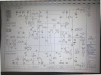
It' a bit late to post this now but just for comparison with Nait5i and the NAP250 schematics, here is a reverse-engineered sketch of the power amplifier circuits in Nait2. It was posted here some 14 years ago by Etsang, with the help of none other than Zen Mod. As you can see, no 27R resistor is used, whether that was a fudged means of altering the thermal compensation in NAP models or not.
That's a little too hazy for my eyes and I'd need to study the reverse side to do better than guess. Back in 2011 at PFM forum, Martin Clark, also a member here, had this to say in reply to a query about the accuracy of the above sketch and others for the associated circuits of Nait2: "the schematics are pretty good. It will work if you build to them, anyway."
Cloning the Nait 2 | pink fish media
Cloning the Nait 2 | pink fish media
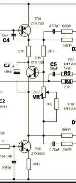
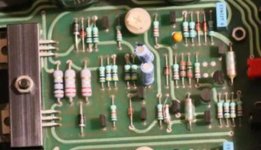
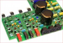
The photo shows 25 resistors and the schematic 24. A 1k resistor is missing. The Nait is a shaved-down NAP, to save cost and reduce its sound quality.
The attached pic is from Stereophile magazine and shows a refurbished Nait 2 board, though the MF resistors shown are original. I count only 23 resistors in either channel. Unless the extras are hiding elsewhere (not underneath) they must either be unusual types of resistor, optional parts or one of our pics is of a revised board.
Edit 2: I understand channel balance was preset at the factory with an adjustable resistor in the NFB path. I don't see any normal type of trimpot there so perhaps those dark brown, upright gizmos in the centre of the board are related to that?
Edit 2: I understand channel balance was preset at the factory with an adjustable resistor in the NFB path. I don't see any normal type of trimpot there so perhaps those dark brown, upright gizmos in the centre of the board are related to that?
Attachments
Last edited:
- Home
- Amplifiers
- Solid State
- NAP-140 Clone Amp Kit on eBay