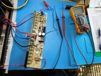
Well, testing is slow going. At the best, it takes me about 45 minutes to set up my test gear and the amplifier sections on the dining room table, and I have limited time to work, hence the delays between recent reports.
First I pulled ZD13 in the protection circuit the right channel and it measured very close to specified 6.8V. I also pulled Q136 and it tested good.
I installed Q116 and Q117 in the right channel board without the heat sink attached, then shorted C106 to maintain zero bias. I checked voltage at R126 and R127 which were +0.2VDC and -0.2VDC respectively.
However, voltage at the test points was -76.9V, indicating a short to ground (I think I made an error in an earlier post and noted a positive voltage). I used a Fluke IR thermometer to check heat levels and found heat building pretty quickly at Q110 and Q111 (2SA1370), as well as Q106 (2SC2705) - about 68C.
There is supposed to be -72.8V (with everything connected obviously) between the bases of Q106 and Q112 (2SC3467), but I measured only 0.70VDC. I shut it down to let everything cool, then fired it up for more measurements. There is supposed to be about +70.8V at each of the emitters of Q110 and Q111, but I had zero volts.
The temperature of QII5 (2SA1306) was really high - 76C, and that has a large heat sink. There was 156V between base and emitter on that device. The complimentary Q114 (2SC3298) was running much cooler.
Should I be focusing on the downstream device (Q115) first, and working my way upstream? I believe I have a replacement, which I hope is not counterfeit.
What is the base voltage on Q110/Q111?
also check B-E on Q110/Q111- should be around 0.6v
What is the base voltage on Q108?
same B-E test
Does ZD12 test OK?
also check B-E on Q110/Q111- should be around 0.6v
What is the base voltage on Q108?
same B-E test
Does ZD12 test OK?
There is supposed to be -72.8V (with everything connected obviously) between the bases of Q106 and Q112 (2SC3467), but I measured only 0.70VDC.
I read the schematic as meaning both the bases of Q106 and Q112 should be -72.8V which would make them 0.6V higher than the emitters and tallies with the stated emitter voltages .
@pwdiya12: Thank you! I'll get to those measurements this morning.
@epicyclic: Ah, yes. I saw the connected arrows and may have misinterpreted it. I'll re-measure - thank you. Also, I did pull both Q101R and L and they tested good and tightly matched, but I'll re-check to be thorough.
@epicyclic: Ah, yes. I saw the connected arrows and may have misinterpreted it. I'll re-measure - thank you. Also, I did pull both Q101R and L and they tested good and tightly matched, but I'll re-check to be thorough.
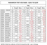
I made up a table for all measurements. I still can't find any component that is shorted or open, but it's clear something is very wrong.

Tested film caps, all good. The electrolytics are new and test good.
Q101 tests good.
Pulled ZD12 and tested - good.
Same with ZD11 - good.
During testing today, Q115 did not get hot, unlike yesterday. I pulled both Q114 and Q115 - they test good.
Tomorrow I'll check voltages on Qs 134,135 and 136.
Scoured the board for bad traces and joints - nothing. Nothing looks burned, none of the resistors test open, shorted, or out of tolerance.
Are all the grounds connected particularly the ground on the input and are they connected to chassis .
I'll be reassembling the chassis and right channel board for more testing today, and will re-check ground connections. There are 3 ground connections to each board - input shield, center tap of the 2 3,300uF filter caps, and the PS ground. These all originate at the PS filter cap/rectifier board, and I know they are connected securely, but your question (same asked off-list by pwdiya12) has me wondering if my ground connection at the input has come loose.
Thank you!
Thank you!
Hey! Some progress!
Thanks to pwdiya12 and epicyclic, I re-examined the signal ground to the input and found that my repeated removal and installation of the board for testing had damaged the thin wire at the terminal. I made a secure extension piece, as well as an extender for the limiter-protector wires to avoid damaging that, and to place the circuit board more securely on my anti-static work mat.
Voltages are now pretty close to expected, though higher because there are no outputs installed.
The best news is I found a resistor that goes to the collector of Q111 that is way out of spec. It was OK when previously tested with my DMM, but I think it was on the margin and developed high resistance throughout this work. It should be 18k and measures 1.23meg. Not sure if that is causing the unexpected collector voltage on Q111 - should be 0 but was -5.77V.
Have to stop to spend the rest of this Sunday with my wife and dogs, and will have to order replacement resistor(s).
Thank you for your help with this. If I can get the board stable, it would make sense to install the other drivers and outputs, correct?


I've done a lot more work to diagnose the trouble, but seem to be making little progress.
First, that 18k resistor was fine; there was residual voltage in the local rail caps affecting the reading. I ended up replacing that resistor on both boards anyway.
I tested all diodes, and lifted legs on the Zeners to test them. Most of those were close to spec, but ZD12, which is connected to the bases of Q110 and Q111 and the emitters of Q108 and Q109, was reading about 4.3V on the left board and 3.8 on the right, as opposed to specified 3.2V.
After ordering and installing all new diodes on the boards, including the current limiting diode D105 (except the 3.2V Zener, which I could only find in SMD), I then replaced Q111 on both boards with 2SA1371 (higher voltage part than a1370), thinking the collector voltage on each was the result of leaky transistors. I also replaced Q112 and Q110 on each board. I also re-tested all resistors, caps and transistors for shorts or opens (none).
After this work, Q111 collector voltage on each board was down to about 1.3-1.5V, but still not 0V as shown on the schematic. I thought that might be because I was running only one pair of drivers and the bias was shorted, so I populated the board with the remaining drivers and the outputs, and tested the left channel board on the DBT. Inputs shorted, connected to grounds, output rail ground and main ground connected, PS rails connected, but speaker output wires not connected.
Unit drew about 0.15A after settling, with no bias, but when I turned up bias, rail voltages dropped from about 77VDC to 64VDC, and protection kicked in when bias reading went above about 25mV, at which time it dropped to about 6mV, though current draw stayed high at 0.5A, even though the outputs were not apparently drawing current. I measured voltages at the bias resistor Q139: E-gnd = .571V, C-gnd = .616V, and B-gnd = 100mV; all readings lower than specified.
None of the output transistors shows shorted, but as reported earlier, many are very low in hFE. No cases were shorted to the heatsink. Clearly, there is something that is pulling rail voltages down however, and collector voltage on Q111 was back up to about 5VDC, when it should be 0V. This doesn't seem to be down to ZD12 being out of spec. I could use some suggestions by any Nakamichi experts about now.
Thank you!
Greg
Forgot to add:
The front panel Limiter board tested good with all parts in spec. On startup, the red protection LEDs come on then switch off when the speaker relays switch on.
However, I suspect there is still HF oscillation occurring because the new 5R1 Zobel resistors get hot quickly with bias reading above a few mV.
Also, offset which was down to about .04mV when I was testing the boards with only the first pair of drivers, now was about 11mV during the left channel board testing.
Thank you - that is the exact part I used. I didn't refer to D105 as a Zener in my post. ZD12 is the 3.2V part I couldn't find in through-hole. I can find a 3.3V.
Cheers.
Cheers.
Check the voltage drop over each and every output emitter resistor as the test point only measures across one , this will show you any variation in the output devices and hopefully any suspect ones .
Well, that didn't reveal very much, unfortunately. None of the emitter resistors showed much voltage drop, though there was variance, because the bias can't be adjusted past a few mV. However, when I do adjust the pot, the bias reading stays about the same, but current draw on the entire circuit goes up, with rail voltages dropping from about 77V to 64V.
Moving to the right channel board, Q110, Q111, and Q112 are all running hot at about 46-47C, while all other components are about 24C. Also R111 is specified at 162k, but has a slightly burned end where the lead enters the body, and there is the beginning of a discolored band, and it measures 57k. I'll change that and re-check. The trouble seems to be originating in this section of the circuit, but I can't find any obvious reasons yet.
Moving to the right channel board, Q110, Q111, and Q112 are all running hot at about 46-47C, while all other components are about 24C. Also R111 is specified at 162k, but has a slightly burned end where the lead enters the body, and there is the beginning of a discolored band, and it measures 57k. I'll change that and re-check. The trouble seems to be originating in this section of the circuit, but I can't find any obvious reasons yet.
" When you adjust the pot the bias reading stays about the same but the current draw on the entire circuit goes up "
This is my point does the bias stay the same on all of the outputs devices
This is my point does the bias stay the same on all of the outputs devices
- Home
- Amplifiers
- Pass Labs
- Nakamichi PA7II serious problems, need ideas, please