Those measurements seem normal.
The fact you have full neg rail showing up on both channels bothers me. It still leads me to think that something is universally affecting both channels. Usually when I see channel failure its rare that both channels exhibit the same symptom unless there is a short but your measurements show there is not a shorted transistor on the output.
With the amp off and fully de-energized measure the resistance between the base of Q116 & Q117. This should be about 20k ohms or so.
I would find some where on the front end of the circuit to verify that you have full +/- rail voltage on the front end side of the 10r resistors R160/R161
Also with the amp powered on measure the DCV at the base of Q114 & Q115.
BTW I'm not sure what you're using to probe the voltages in the active circuit with but if you're using a standard set of DMM probes with the long bare tips I'd insulate them by wrapping a small bit of electrical tape around them leaving just the very tip of the probe exposed. This will save you a lot of heartache if the probe slips. Take it from someone who has experienced that heartache firsthand.
I'm in the mid-cities area between Dal & Ft Worth.
A drink would be great! 🙂
I'm using a Fluke 115 with the standard probes. Great idea on the electrical tape. I've added some heat shrink material to prevent sparks from flying when the probes slip.
with the amp powered off:
Q116L to Q117L base measurement: 2.227k
Q116R to Q117R base measurement: 2.578k
So, 10x lower than what your were expecting.
With the amp powered on, I can measure the +/- rail voltages at the Q114 and Q115 collectors. I probed all the pins on these transistors for completeness.
Q114L
C: +77.3v
B: -77.2v
E: -76.7v
Q115L
C: -77.3v
B: -77.2v
E: -76.7v
Q114R
C: +78.1v
B: -77.2v
E: -77.4v
Q115R
C: -78.1v
B: -78.1v
E: -77.6v
So it looks like the rails are ok as measured on these transistors too. Should I probe the transistors between Q114/115 and the input connector next?
Okay looking again at the bias network shows 2 - 3k ohms is about right for the Q116/117 resistance.
I'm interested now in what DCV you measure at the base of Q112?
I'm interested now in what DCV you measure at the base of Q112?
The combination of R113/114/115 & D105 is a current regulated voltage divider network which should give you around -60V (in ref to gnd) on the base of Q112. But you are also measuring full rail voltage on the collector of Q112 from your earlier measurement so I would power down and check the resistance from C - E on Q112 to see if its shorted. This short would also explain the full rail voltage on the base of Q112.
It's possible the voltage divider I just mentioned is not conducting but this wouldn't explain the full neg DC rail on the collector of Q112. To me only a shorted Q112 or Q115 explains this. Even if q112 is shorted I'd still check that divider to make sure its dropping voltage across R115. The DCV across R115 (100k ohm) should measure well over 100V if that network is working properly. If its not then I'd suspect D105 which is a 1mA current regulator diode.
It's possible the voltage divider I just mentioned is not conducting but this wouldn't explain the full neg DC rail on the collector of Q112. To me only a shorted Q112 or Q115 explains this. Even if q112 is shorted I'd still check that divider to make sure its dropping voltage across R115. The DCV across R115 (100k ohm) should measure well over 100V if that network is working properly. If its not then I'd suspect D105 which is a 1mA current regulator diode.
Q112L C to E: 5.56M
Q112R C to E: 3.579M
Hmm, definitely not shorted, but perhaps something else in circuit is making it seem as if it's not shorted?
Before powered on, I did a diode check on D105:
D105L: 0.700v
D105R: 0.640v
With the amp powered on, measuring across R115:
R115L: 95.0v
R115R: 111.6v
the 95v seems out of place.
voltage measured on +rail side of R115L: 78.5v
voltage measured on +rail side of R115R: 78.6v
voltage measured on diode side of R115L: -16.05v
voltage measured on diode side of R115R: -31.9v
Seems like at least the left channel diode might be shot despite the reasonable diode check voltage?
So the R115 voltages sound within reason. That works out to .95mA on the L and 1.1mA on the right which are prob within spec for that diode even if it's going to give some differences between channels. Anyway that's not your problem.
I should've told you before but check Q112 for C to B and B to E for shorts.
I should've told you before but check Q112 for C to B and B to E for shorts.
At the same time I did the C to E measurements, I measured Q112 C to B and B to E but didn't note them. They were in the 2-5Mohm span, no obvious shorts to me. But I've definitely had issues in the past where shorted transistors didn't measure as shorted until I removed them from the circuit.
I was going to suggest that you may need to remove these from the board and put them on a transistor tester. Or at least perform a diode test with your DMM on the junctions out of circuit.
I don't have a transistor tester, but I can check for shorts and do the diode test. Are there any parts other than Q112 I should pull while I have the desoldering iron out?
And, when working on these beasts, do you normally bend the PCB back to allow access to the back side of the board? That seems fine once or twice, but eventually that could stress the leads on the transistors. On the other hand, if I remove the transistors from the heat sinks, I could damage the sil-pads or the transistors themselves.
And, when working on these beasts, do you normally bend the PCB back to allow access to the back side of the board? That seems fine once or twice, but eventually that could stress the leads on the transistors. On the other hand, if I remove the transistors from the heat sinks, I could damage the sil-pads or the transistors themselves.
I have one of these gadgets, its great to have around.
I know its a pain but I'd just remove the board from the heatsink to avoid damaging any transistor leads.
I'd also remove Q115 and check it as well.
I know its a pain but I'd just remove the board from the heatsink to avoid damaging any transistor leads.
I'd also remove Q115 and check it as well.
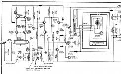
Well I've been looking at the left ch schematic all this time and didn't realize that the right ch schematic has the voltage measurements on it. Doh!!!
I would check all of those resistors located around those transistors also. R110, 111, 112, 113.
I would check all of those resistors located around those transistors also. R110, 111, 112, 113.
Resistors measured in-circuit:
R110L: 1.095k ok
R111L: 162.5k ok
R112L: 149.0 ok
R113L: 1.32k ok
R110R: 1.097k ok
R111R: 162.2k ok
R112R: 149.0 ok
R113R: 1.2k ok
Transistors removed from circuit:
Q115L (PNP):
Resistance Check
B to C: 5.53M
B to E: 5.97M
C to E: OL
Diode Check per https://vetco.net/blog/test-a-transistor-with-a-multimeter/2017-05-04-12-25-37-07
B to E: OL ok
B to C: OL ok
E to B: 0.621v ok
C to B: 0.613v ok
C to E: OL both directions ok
Q115R (PNP):
Resistance Check
B to C: 3.6M
B to E: 5.89M
C to E: OL
Diode Check
B to E: OL ok
B to C: OL ok
E to B: 0.622v ok
C to B: 0.612v ok
C to E: OL both directions ok
Q112L (NPN):
Resistance Check
B to C: OL
B to E: 6.9M
C to E: 5.36M
Diode Check
B to E: OL not ok
B to C: OL not ok
E to B: 0.690v not ok
C to B: OL ok
C to E: OL ok
E to C: 0.683v not ok
Q112R (NPN):
Resistance Check
B to C: OL
B to E: 6.8M
C to E: 3.5M
Diode Check
B to E: OL not ok
B to C: OL not ok
E to B: 0.685v not ok
C to B: OL ok
C to E: OL ok
E to C: 0.674v
So it looks to me like Q115 is ok in both channels, but Q112 is bad in both channels. I am confused why I'm getting a voltage drop in cases where I should see OL. It seems like failure modes for transistors should only go from having a voltage drop to NOT having a voltage drop.
I see some people recommending the KSC3503 as a replacement. It's a different package, but it might fit. Thoughts?
Q112 is just a current source passing about 4mA. The selection of the 2sc3467 was most likely due to the fact it was a readily available high voltage 1W transistor. For this reason the KSC3503 should work fine if you can fit it in and the higher voltage rating and the slightly higher Pd will be a plus. The ZTX657 is also a good fit size wise but would require swapping B & C legs.
I'm not really sure why Nak chose to use the D105 (E-102 CRD) in the manner that they did and not just use a pair of diodes like they did on the current source (D103/D104) for the input LTP. The only reason I can think of is that Nak is using this as a slow DC rail bleed off after power down. There is no added DC rail bleed resistors anywhere. Maybe someone else more knowledgeable will chime in as to whether there's another reason they chose this CRD instead of a pair of diodes for this current source voltage reg.
Either way I would replace both of the CRD's while you have it apart.
Attachments
One thing I forgot to mention is that R113/R114 are in parallel so you should measure 1.21k across R113. I notice that you measured 1.32k across R113L, this should mean that either R113 or R114 resistance is out of spec. You will have to check them with one leg lifted.
Ok, with the resistor legs lifted, I measure 1.33k on R113L and 13.29k on R114L. I'll replace R113L since it's out of spec.
Looking at the schematic again, I get your point. R113 should be 1.33k, but the two resistors in parallel should be 1.21k. Maybe there was a bad solder joint? I'll reresolder and see if there's a difference.
Resistors are soldered back in place and I'm now getting 1.2k for the parallel network for both PCBs. Before I started work this morning, I remeasured the left board and definitely still got 1.33k for R113L. Looking at the right channel, I see there's a solder bridge on one side of that resistor pair, but there wasn't on the left channel. There must've been a PCB routing error that was meant to be addressed with a wire or solder bridge, but that didn't get done on the left channel for some reason. Very strange!
The missing solder bridge was probably an oversight by the person that assembled the board originally. It doesn't doesn't like much of a shift in resistance but that small shift in resistance took the current through Q112 up from 4mA to about 4.8mA which also moved the power dissipated by Q112 up by 20% as well.
I'm still trying to get my head around how Q112 would have failed in both the left and right channel especially when only one channel had shorted output devices in it. To me this points to a deficiency in the circuit that allowed a failure of Q112 in both channels when the transformer was heavily loaded in the second or so it took the main AC fuse to blow when the R-ch outputs shorted originally.
I'm still trying to get my head around how Q112 would have failed in both the left and right channel especially when only one channel had shorted output devices in it. To me this points to a deficiency in the circuit that allowed a failure of Q112 in both channels when the transformer was heavily loaded in the second or so it took the main AC fuse to blow when the R-ch outputs shorted originally.
Does your amp happen to have the Zener added in across D104 & D103? As shown in the schematic I posted earlier. This is showing as a Canada only addition.
- Home
- Amplifiers
- Pass Labs
- Nakamichi PA-7II won't power on, limiter resistor blown