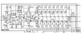
Here is the schematic of the PA 7 nakamichi amplifier
Noticed that the LTP doesn't get any feedback from the output
Can somebody explain why ?
can somebody comment that in terms of sound quality ???
After that there is couple of more questions ....
in basic terms and except the feedback thingy this shares similar principal of operation with the ESP design p68, at least for the output schem.
Now Rod in his article suggest this amplifier for sub woofer use since there some concideration about crossover distortion or poor freq response , even though it is clearly stated that he didnt notice anything while listening to the amp .
So i wonder if a similar problem applies for the PA7
Then again there is a bit of wierdnes in the design since the amount of outputs is pretty high for 60 V rails .... I understand that this apmplifier with that ammount of outputs will easily drive any load regardless of the speaker impedance .
In the PA7 i also notice fairly hi ballast resistors 1R that also is a question
Thank you very much
Attachments
do a search for this amp and also "stasis" to get info on how it works. you'll find answers to all your questions in those threads, some answered by Nelson Pass himself. If you don't know already, you'll find out why I mentioned him when you search. 🙂
Yes, this is the very basis of how the Stasis design concept works.
It works better with 8R speakers that have more flat impedance curves. Lower impedance loads create variations that because the outputs are open loop, are not corrected. Every design concept has pros and cons. These are the cons for Stasis.
For sound quality, again pros and cons. It is a very good sounding amplifier.
I'm not going to comment or compare with another design, I do know this one very well. The 1R0 emitter resistors are important to keep the outputs more linear. Remember they are open loop.
Οκ i am familiar with the design and the designer
rememeber that its quiet highly biased at 40 ma per transistor
yes then ballast resistors and asking very litle from every transistor makes the all picture complete
Thanks all
rememeber that its quiet highly biased at 40 ma per transistor
yes then ballast resistors and asking very litle from every transistor makes the all picture complete
Thanks all
I forget the bias level in the manual, but I wouldn't call it highly biased compared to many amplifiers out there. I know of several BJT output amplifiers biased at 50 mA per device and much higher. Mosfet designs run from at least 50 mA to 250 mA for A-B types. Yes, bias has to be higher than the 20 mA we see often, but it isn't that high in the grand scheme of things.
That amp doesn't try to reduce cross-over distortion from the output section using feedback, so its going to much less performant than it could be, for inscrutable reasons. Primarily the THD and damping factor specs will show up these shortcomings.
Its a straightforward CFP output section, feedback is taken from the driver section rather than the output as would normally be done (avoiding the risks of instability of CFP outputs which can be tricky to stabilize sometimes). CFP outputs tend to be reasonably linear, but the crossover artifacts are spread right across the spectrum unfortunately.
For some strange reason 2SC3333's are used in zener mode, rather than zeners or LED strings, for biasing parts of the input. The behavious of base-emitter junctions in zener mode is poorly characterized and probably subject to more variability that using the normal approach.
The number of output devices seems profligate, although there is some evidence that multiple devices can reduce cross-over distortion by averaging out slight different responses of the individual devices. It will also defend against secondary breakdown - so perhaps the thinking is buy 8 pairs of output transistors once, rather than buy new sets every time they blow-up... And more outputs may help with the damping factor a little.
There is a neat avoidance of an electrolytic in the feedback network, at the expense of a large expensive 10uF 200V film cap.
Hi Mark,
CFP stages can perform better than some people think they do.
Reverse biasing the e-b junction is not uncommon. It comes down to price I think. Nelson does experiment with parts on his own, so I am certain he was satisfied with the consistency of breakdown voltages. The Japanese engineers at Nakamichi would have confirmed his findings. If it were critical they would have used an instrument grade voltage reference (I'm thinking of a 6.9 V reference, you should know which).
The large number of output devices does a lot of things. Delta I per device is reduced, output impedance is reduced and they tended to match beta well. My own tests show that they work better matched for distortion, so averaging out variations doesn't seem to be correct. When the stage is outside the feedback network as this is, you want a linear output section. So high numbers of devices with a 1 ohm emitter resistor suits that bill nicely.
I only ever saw one PA-7 II blown up. It was under warranty and a copper shipping staple killed it. It killed the staple back - like in two pieces with a melted area missing - lol! I replaced all the output transistors with a matched set. Right to the present day, I have never seen or heard of another with blown outputs.
The reasons for taking the feedback earlier on is simple. Nelson was trying to reduce the impedance variations hitting the Vas from the load. Simple. So the reason for this arrangement was done with careful consideration. Deliberate. It is one solution to this issue, not the only one and not best in all situations. But, there was nothing wrong with this approach.
-Chris
- Home
- Amplifiers
- Solid State
- Nakamichi PA 7 questions