in the attached PDF you will find my own drawing of NAD's PP3 (PP-3, Phono Preamp 3), except the AD-converter section with PCM2905; the genuine diagrams are not available about NAD.
Unfortunately I don't understand the complete circuit - especially concerning certainly devices I don't know the exactly aim:
1) R181-R184, D101-D102 and R169-R170 (Voltage Regulator)
2) R150-R152, C138-C140 (RIAA-network, right channel and according devices left CH)
3) R156-R158, C154-C156 (RIAA-output, right channel and according devices left CH)
Additional I don't find a datasheet on the web for the device near by USB output. The SMD marking code is "RT93" (outline you will find in the attached pdf by the device numbers).
Who knows more about this device?
And a last question: The German PP3 folder mentioned a special circuit topology to realize a soft clipping function. Which devices are therefore in use? Thank you for your hints.
Some URLs for your information:
NAD PP3 folder
NAD Electronics :: PP-3 Digital Phono Preamplifier
Instruction Manual
http://nadelectronics.com/content/100702111631-NAD_PP3_DIGITAL_100628.pdf
Schematic NAD PP2 (PP 2 Phono Preamp 2) for comparing to the PP-3: by post #6 about
http://www.diyaudio.com/forums/powe...2-three-terminal-fixed-voltage-regulator.html
Attachments
Last edited:
Finally(!) here's a Reply for you ! Thanks for the schematic - there does not seem to be an official one available, even to official service centres.
I gather they are unreliable little beasts - My first one outputted a large buzzing noise on top of all audio, and now my replacement has died (no Power LED). Should be relatively simple to fix now (thanks).
RTL93 ? Mine does not have this installed - just a bunch of unpopulated pcb pads in the area !
Cheers
PCB Layout wanted
From a friend I got this phono part and I did not remember that I create a schematic of it and uploaded it here.
No output signal is present at both channels, both at MM and MC input.
The reason therefore is clearly too low voltages (+2/-5VDC instead +9V5/-9V5DC)
Next step is disconnect the voltage regulator from the actually gain stages to find the reason in detail - for that I have to cut the voltage traces at the right places.
Maybe a SMD chip capacitor have a transition between the voltage rails and GND.
Without a PCB layout the component in question (fault-causing component) is hard to find.
Maybe one of the members can upload this.
Thank you very much.
P.S.: I don't know the usual colloquial term for what I need, so I have attached a PDF file from a PCB layout of another audio device that shows what I mean.
Attachments
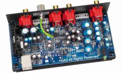
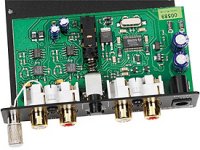
I just note, that there are at least two PCB versions on the marked - do to the attached images. I need the wanted PCB layout from the old version of first image (from the year 2008) and not from the second image (currently version - so I thinkl).
Attachments
Another option that would help would be a faulty PCB (mainboard) from NAD's PP-3. Maybe one of the member can make an offer therefore.Without a PCB layout the component in question (fault-causing component) is hard to find.
Maybe one of the members can upload this.
Thank you very much.
- Status
- Not open for further replies.