I replaced the dubious looking TIP32's with a more decent one. and also replaced the IRF9610 with IRF9640. still having trouble with the DC offset. although on the other channel, the foil pad for the source resistor for the 9640 tore off and I blew all four output devices. I have to get new ones before resuming work on the amp.
djQUAN: If you want you are welcome to send your board to me in Denmark, then i will repair it for you, and investigate the DC problem too. ..
You can find the address by clicking on the link below
Lars
You can find the address by clicking on the link below
Lars
I would like to but the heatsink is quite heavy (well, most are mounted on it but I could remove them and send the two separate boards instead) and I'm not sure how much it will hurt my wallet. 
anyway, I'll contact you if I run out of options and decide to send it over. also, how much would it cost me? (other than the shipping....)
anyway, I'll contact you if I run out of options and decide to send it over. also, how much would it cost me? (other than the shipping....)
PCB Board
Hello again,
i read this thread at the beginning and now i want to ask you,
if there is a PCB Board av. for us / me.
 Can anybody sel my 1 or 2 boards ?
All the best
- uwe
Hello again,
i read this thread at the beginning and now i want to ask you,
if there is a PCB Board av. for us / me.
Can anybody sel my 1 or 2 boards ?All the best
- uwe
Uwe: Since there is some discussion still about the source resistors, i have decided to make a PCB with single output devices. Using the right output MOSFET's you can produce up to around 500 Watts RMS power.
And since single devices sound better than multible devices, it will be great for audio use, and not only for PA.
Maybe someone else is doing the PA board ??
And since single devices sound better than multible devices, it will be great for audio use, and not only for PA.
Maybe someone else is doing the PA board ??
Thank you Lars,
i don't ave any PA. I want to drive two KEF B-139B /Subwoofer/.
So 100W-150W is enough for me.
I stop now the handmade Zeta without a PCB.
I read straight the "discussion about the source resistors" and
think a 0 Ohm (bridges) can solve the problem/ discussion.
in the last tow weeks i build the mono "ZETA" from Susan Parker.
Now i hear a live concert from "Herman van Veen - in echt"
so far, i will read again ...
- uwe
i don't ave any PA. I want to drive two KEF B-139B /Subwoofer/.
So 100W-150W is enough for me.
I stop now the handmade Zeta without a PCB.
I read straight the "discussion about the source resistors" and
think a 0 Ohm (bridges) can solve the problem/ discussion.
in the last tow weeks i build the mono "ZETA" from Susan Parker.
Now i hear a live concert from "Herman van Veen - in echt"
Lars Clausen said:Uwe: Since there is some discussion still about the source resistors, i have decided to make a PCB with single output devices. Using the right output MOSFET's you can produce up to around 500 Watts RMS power.
And since single devices sound better than multible devices, it will be great for audio use, and not only for PA.
Maybe someone else is doing the PA board ??
so far, i will read again ...
- uwe
Lars Clausen said:djQUAN: Nothing of course 🙂
😀 😀 😀
I'll try to check out how much it will cost me to ship the unit without the heatsink....
just for a little curiosity, I removed the 20k (originally 100k)feedback resistor from the speaker output and connected it to the collectors of T9 and T10 and there, I got 140mV offset measuring at that point. I'm not sure if the next stages are causing the offset or T9 and T10 are just loaded so the voltage is lower......
also, I'm only having the problem when the supply voltage is +/-50V. when I decrease it to +/-25 (plugging the 220V primary to 110V) offset with the entire circuit is an acceptable ~100mV.
once I get these two channels running, I'll go ahead and design the one with 4 pairs of outputs per channel running at +/-70V.
Lars
Please reply to my posts , 254 & 258 and obliege .
Dj Quan
check if any of the devices is leaky in the input stage , as there is no problem in the design , it is working fine here .
Please reply to my posts , 254 & 258 and obliege .
Dj Quan
check if any of the devices is leaky in the input stage , as there is no problem in the design , it is working fine here .
Ampman,
After your Very Serious And Very Experienced statement that Rsource does nothing at all, I conducted a Very DIY and Very DIY research.
Firstly, I still vote for putting Rsource/RE for realibility.
I take Vmosfet (IRF240 pairs), Bipolar (C5200 pairs), and Lmosfet (K1058 pairs) output stage.
Bipolars have the biggest gain. Vmosfet has lower gain than bipolar. Lmosfet has the lowest gain.
Vmosfets seems to have "Virtual internal Rsource" that makes the gain low.
So, if you put these for output stage in parrarel, it is quite acceptable if you dont use Rsource. Why? Because they inherently have Rsource.
But still, putting outside Rsource will add the realibility more.
I think if you use Lmosfet, it will be more tolerant to "not using Rsource", but you won't be able to use parrarel bipolars without RE, due to very high gain of each device.
LC, have you been checking your personal email?
rajeev luthra said:Lars
Please reply to my posts , 254 & 258 and obliege .
Dj Quan
check if any of the devices is leaky in the input stage , as there is no problem in the design , it is working fine here .
how do I do that?
Dj Quan ,
It could also be lower working voltage of a device , as you say that the offset is normal at low voltages , try the test you did with higher voltage by connecting the feedback resistor at col of t9 &10 and disconnecting the vas,
if the problem is there try replacing the transistors , normally leaky devices show resistance between col & emitter
Source resistors yes or no ,
Source resistors yes or no ,
After reading the comments of ampman and other friends I realise that
this issue is more complicated than what it looks like , as so many
factors are involved , there can be variations in so many places , 100%
of device matching is difficult , equal power and current sharing amoung
parallel devices, the device temp at various power levels of the amp ,
voltage rating , high voltage rails , extra space on the pcb , etc etc
I am in the repairing field and I have many times replaced only one
mosfet from a bank of mosfets , however it is difficult to reason the
cause of failure of the device .
I hope those who have more experiance with mosfet amp design could
give their opinions .
Thanks
all the devices I used are 100V and above.
the test that I mentioned in removing the feedback and connecting to the collectors of T9 &10, I did that test at +/-50V, although I did not try it with +/-25V.
all the decvices that I used are brand new and bought the same day (input stage devices). is there a possibility that my PCB layout could be the cause? I don't know how to post my layout as I did everything by hand. it is weird as I have both channels having the smae problem. I also have another two boards assembled but haven't been tested yet.
I don't have time today so I'll try to remove all small signal transistors and test for leakage next week.
Hey Rajeev; Source / Emitter resistors
I have built amps that use source resistors in the output stage and amps that don't.
I built a few amps based on an altered quasi-complimentary Elektor design around 12 years ago using Philips BUK437-400B power FETS. In this amp there were no source resistors and I used closely matched FETS. Whilst these FETS were well matched on the bench in the dynamic environment of the cct the current was not shared equally. In practice this was not a problem, though I hoped that the FET dissipating most of the heat (up to 14 watts idling) wasn't the furthest from the thermal detection diode.
Since then all of my amps (including the same amp modified) have used source resistors for the following reasons.
1. Better current sharing, plus the quiescent (bias) current through the output stage is better stabilised under differing conditions.
2. A fixed and constant resistor added to the Rds-on of the FET makes for a more linear stage.
3. Depending on the output stage setup, the small voltage drop across the source resistor can provide local feedback to the gate drive, further improving the linearity of this stage. In my latest design this works as follows.
As the current increases through the source resistor the gate to source potential is decreased. This tracking (or feedback) would not work without the source resistor.
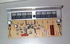
A bit of a jumbled response, I hope some it is understood. A piccy below of the amp module I described above.
Cheers
PS. The BUK437-400's were a real sweet FET. Curse you Philips for stopping production.
I have built amps that use source resistors in the output stage and amps that don't.
I built a few amps based on an altered quasi-complimentary Elektor design around 12 years ago using Philips BUK437-400B power FETS. In this amp there were no source resistors and I used closely matched FETS. Whilst these FETS were well matched on the bench in the dynamic environment of the cct the current was not shared equally. In practice this was not a problem, though I hoped that the FET dissipating most of the heat (up to 14 watts idling) wasn't the furthest from the thermal detection diode.
Since then all of my amps (including the same amp modified) have used source resistors for the following reasons.
1. Better current sharing, plus the quiescent (bias) current through the output stage is better stabilised under differing conditions.
2. A fixed and constant resistor added to the Rds-on of the FET makes for a more linear stage.
3. Depending on the output stage setup, the small voltage drop across the source resistor can provide local feedback to the gate drive, further improving the linearity of this stage. In my latest design this works as follows.
As the current increases through the source resistor the gate to source potential is decreased. This tracking (or feedback) would not work without the source resistor.
A bit of a jumbled response, I hope some it is understood. A piccy below of the amp module I described above.
Cheers
PS. The BUK437-400's were a real sweet FET. Curse you Philips for stopping production.
Attachments
DJQuan,
Why dont you try to ground the input, and measure the voltages. Disconnect the output stage first. Is the offset occurs after the VAS? You can search the origin of the DC offset by calculating the voltage drops on resistors, are they similiar to the voltage drops calculated in papers? Usually DC offset comes from a broken device, it could be transistor, resistor or capacitor, that makes the whole cct doesnt work properly.
To make ZETA complete DIY amp, I hope LC gives another schematic with the correct voltages at important points, also a note about how to set bias. This will make the DIYers have a clue if they have something going wrong.
Source Resistors
I agree with Quasi and his reasons. I have been involved with power amps for over 35 years and they make me more comfortable in Cass AB circuits. If nothing else, they make the turn on point for the bias more linear.
That said, I have been working almost exclusively for the last four years in Class D and there, we don't use source resistors. Mind you, even in a 1000W amp, we don't parallel devices either.
Rather than repeat Quasi's points, for a Class AB design, I will just state that I do prefer to have source resistors. If nothing else, they make monitoring the current for the protection circuits easier.
Class D amps;
Yes DM; In class D amps where the FET is either fully on or off, no current sharing resistors are required. With "full" gate drive all of the FETS will be turned hard on anyway.
Hmm....1000 watts with one pair of FETS .....😉
Cheers😎
Yes DM; In class D amps where the FET is either fully on or off, no current sharing resistors are required. With "full" gate drive all of the FETS will be turned hard on anyway.
Hmm....1000 watts with one pair of FETS .....😉
Cheers😎
1000Watts with one pair of MOSFET? Thats something.
I saw a commercial product that uses complementary output. It uses IRF640 and IRF9640 in parrarel. Interesting is that IRF640 is only 3 in parrarel, while the IRF9640 is 5 in parrarel. Unbalanced number of device in N and P output transistors.
I saw a commercial product that uses complementary output. It uses IRF640 and IRF9640 in parrarel. Interesting is that IRF640 is only 3 in parrarel, while the IRF9640 is 5 in parrarel. Unbalanced number of device in N and P output transistors.
Re; 1000Watts with one pair of MOSFET? Thats something.
Hi Lumanauw,
Yes 1000 watts with one pair of FETS is something, but no real big deal to a low Rds-on FET.
The following is quite simplistic but it gives the picture and it assumes one FET when there is always (usually?) another on the other rail.
Let’s take a typical device IRFP360 and see how it goes.
Specs are 400v / 23A / 280 watt / Rds-on 0.2ohms.
Amp rails of +/- 130 volts.
First we look at the instantaneous peak currents and dissipation.
130 volts / 8ohms = 16.25 amps x Rds-on 0.2 ohms = 3.25 volts = 52 watts across the FET. This is well below the 280 watt rating of the FET. This is a worse case instantaneous situation.
In real life there are additional switching losses so the FET's dissipation might be a bit higher, but note also that we are talking about instantaneous dissipation not average. Average dissipation could be a great deal lower.
ok...130 volts * 0.707 = 91 volts / 8 ohms = 1,035 watts RMS provided your power supply is up to it.
So why aren't all amps class D? Many high power PA amps use class D because they weigh a lot less (no big heatsinks, switchmode supplies for some of them too). For audiophile Hi-Fi, many say that specs like noise, distortion and damping factor aren't good enough....but I suspect it's a matter of time.
Moderators; I'll understand if you shift this post.....
Cheers..
PS. If I told you how to suck eggs, a thousand apologies.
Cheers again
- Home
- Amplifiers
- Solid State
- N-Channel mosfet amplifier schematic needed