As far as I remember not far ago (last year) Nelson wrote something about using N-channel JFETs with positive Vgs in an amp design?
Now I can't find it?
I want to read it again......unless I was just dreaming?
I have often wondered what happens as published curves always stops with Vgs = 0?
Can we see curves when Vgs goes positive?
I expect Ids to exceed Idss.......and if handled correct the JFET will stay alive......
I think I actual tried it using the DCR 75 pro tester (by accident) and I think curves just continues but want to know a bit more theory about this.
Beyond the J fringe.
https://www.diyaudio.com/community/...ass Labs-,Beyond the J Fringe,-Thread starter
https://www.diyaudio.com/community/...ass Labs-,Beyond the J Fringe,-Thread starter
So if I have a circuit where Vgs goes positive then I can design a gate resistor that limits gate current to be less than what the device can handle.
It requires that this value is specified in data sheet. Will look for that. I might also just make the gate resistor "large enough".
The "project" is an AC-driven tube tester I might try using for matching JFETs. The tester will peak into positive grid voltage. It is made for 9-pin noval type tubes like ECC83 etc. and uses 220V anode voltage. It can be reduced using a vario in front. So this was the main reason asking for the article.
If someone has an idea for nice universal "sockets" for small signal JFETs I would like to know. Maybe 6-pin DIL sockets can be used.
Forward bias of jfets is good to about 2 x the idss and this is the peak figure, and lower than where the Gate starts conducting significantly. Exceptions ? The SiC Semisouth R100's are used with positive Vgs. Offhand I don't know of any others.
Ok, so it is the max. ids I should design after which makes sense. If I use a like 100k gate resistor the gate itself should be protected I guess against to high gate current when Vgs goes positive.
What is the largest practical value for a serial gate resistor for a small JFET?
It should be able to drive the gate capacitance?
In my case the AC on the gate will be 100 Hz ripple so very slow. Then I might be able to use a rather large value for the gate resistor?
I want to limit the gate current when Vgs gets positive.
It should be able to drive the gate capacitance?
In my case the AC on the gate will be 100 Hz ripple so very slow. Then I might be able to use a rather large value for the gate resistor?
I want to limit the gate current when Vgs gets positive.
There is gate capacitance and current to consider. Most of the time I keep the value below 10k.
The gate current involved is tiny and mostly linear, so why worry about it?
The gate current involved is tiny and mostly linear, so why worry about it?
It was just to be sure the gate current will not damage the device if Vgs gets positive (if JFET gets forward biased by the test equipment).
I spent a year in the 1980s designing full custom digital circuits using Gallium Arsenide MESFETs. The basic transistor was a JFET whose gate/source and gate/drain diodes were Schottky. We didn't fret much about forward biasing these diodes, and for speed reasons, we never installed gate resistors. Although the gate/source and gate/drain junctions were incredibly tiny (10 microns by 3 microns), you couldn't damage them from forward bias in nosebleed speed digital circuits. We even used E/D "super buffer" circuits, which operate a depletion mode MESFET as a source follower. And that is a guaranteed way to forward bias the gate/source junction. No problem.
Thank you for this information. Then the only current to worry about is Ids and off course max Vds etc.
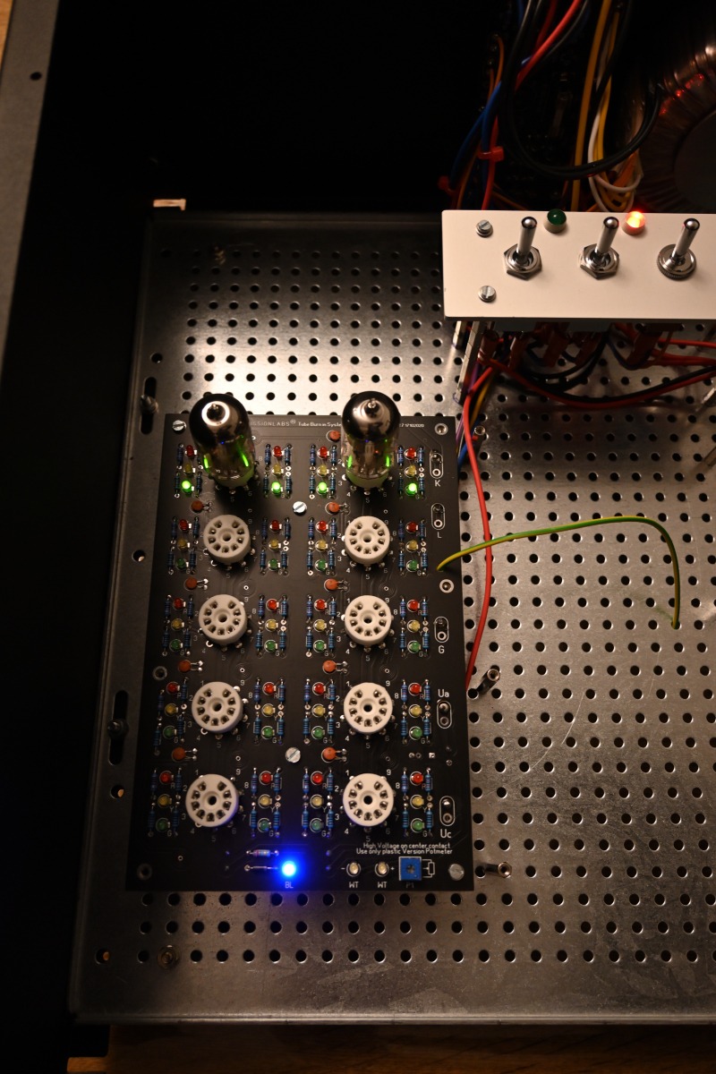
So far the tube burn-in tester looks like this. Bias is adjusted via a 10-turns pot which is not visible in the picture.
A PCB overlay will be installed so only socket and LEDs are visible. The idea is to match via LED light emission.

So far the tube burn-in tester looks like this. Bias is adjusted via a 10-turns pot which is not visible in the picture.
A PCB overlay will be installed so only socket and LEDs are visible. The idea is to match via LED light emission.
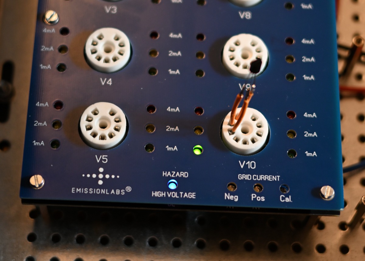
I got one board finished and made a quick test using a JFET with very reduced mains voltage. The concept works but I think I need to make a dedicated tester for JFETs. The idea is to test many and group them. I have got some ideas. Here a J113 is under test. -0,9 Vgs was the most "positive" I could get without a slight modification. Therefor Ids is only in the 1mA range.

There are some similarities between triodes and JFETs........
There are some similarities between triodes and JFETs........
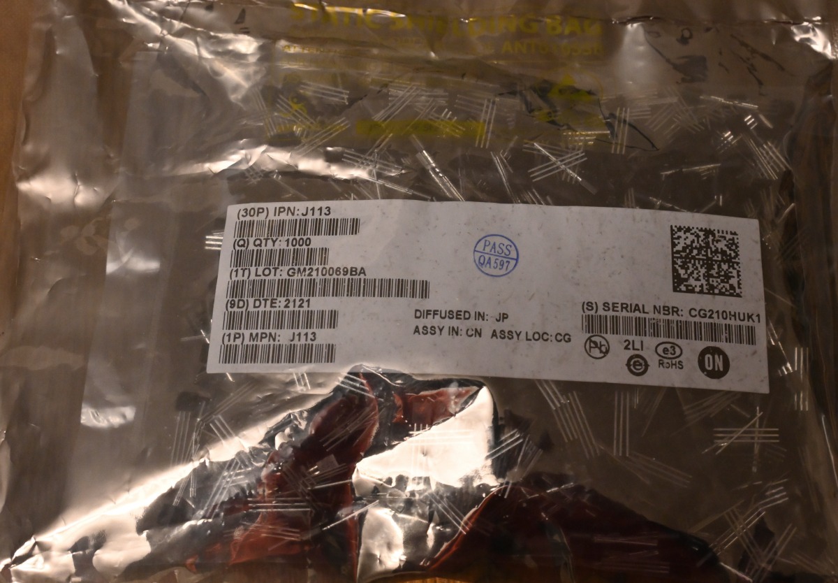
Still possible to get JFETs and get them within a few days........1000 x J113.....and very cheap:

Wonder how many are needed for a 2 x 1000 JFET amp if JFETs needs same Idss.........
Wonder how many are needed for a 2 x 1000 JFET amp if JFETs needs same Idss.........
- Home
- Amplifiers
- Pass Labs
- N-channel JFET and positive Vgs