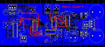
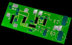
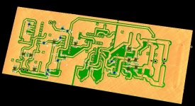
Well, the PCB is now nearly ready.
I haven't included the output filter, and the design is mainly throgh-hole but some SMD capacitors and all the low-power resistors. This way it will be easier to build and tweak. Perhaps in the future I will design it completely SMD.
The analog part (until the first level-shifting transistor) has a GND copper plane and the power stage another one, both of them joined only by a small track.
I have tried to keep the power tracks as short as possible, if you want, you can have a look at the board here:
Attachments
Looks nice! I hope the paracitic capacity at the collector of the second voltage-translating transistor isn't too high.
Regards
Charles
Regards
Charles
hi ssanmor!
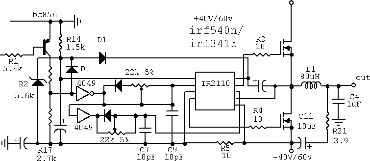
A) Sorry, but I see out a fatal error in your voltage shifter circuit (q4; q1 etc) ~ 50Vp-p for 4030 expected...
B) ir2110 pin 2 and 13 together... it ` s a good idea for low frequency and <1A current or C9*C11*10.
see also (80Khz 200-400w SUB class D amp) http://amploid.narod.ru/pics/2110.gif
C) IMHO self-oscillating modulator topology are rules (for analogue class D), anyway it my modest experience: THD/100 EXPENSES/3
Regards.
Why do you say that, Charles? Due to the track in the PCB or the inputs of the XOR gates?
Best regards
Best regards
Hi Sergio
Due to the track -length and -area. But you will have to experiment and play around with your amp anyway. So I wish you both: good luck and great fun !
Another mod you might want to try is to use a shielded cable for the feedback signal instead of the trace shown.
Another hint: For the first startup take it into service without output devices and without the feedback resistor, just to see if the modulator and drivers work O.K. (the high-side driver has to be "grounded" to work without output devices, but don't forget to remove this connection again afterwards). Then test it with the output devices but still without NFB. If everything is O.K. add the feedback resistor. This way you are able to see where anomalies come from (if there are any at all!).
Regards
Charles
Thanks, IVX, but... could you be more explicit?
What is the error in the level shifter you have seen? The design is simulated and the signal at the input of the 4030 switches between -35 and -50V, so 15Vpp.
What happens with C9,10,11 and the connection between pins 2 and 13 of the IR2110.
And... the link you have provided doesn't seem to work. Could you provide another way to view that image (can be very interesting)
Charles, what do you mean with "grounding" the IR2110 high side driver for the test? I suppose you mean connecting VS to -50V, is this OK?
Thanks for all your help.
I'd suggest to substitute the low-side mosfet by a short between drain and source for this test. This way you won't forget to remove it as soon as you install the mosfets.
Regards
Charles
Regards
Charles
Hi All...
Attachment missing and missing again... please try insert url to your browser an address line. And of course my post*145
was it`s not understandable without IMGAttachment(http://amploid.narod.ru/pics/you_can_synchronise.gif). Sorry for my haste.
Attachment missing and missing again... please try insert url to your browser an address line. And of course my post*145
was it`s not understandable without IMGAttachment(http://amploid.narod.ru/pics/you_can_synchronise.gif). Sorry for my haste.
2 ssanmor
<the design is simulated and the signal at the input of the 4030 switches between-35 and-50V, so 15Vpp.>
pay your attention on D40(clamping to vdriver rail) of Crest lt schematic,
and caps on the - / + HT rails is almost 10000uF per channel,
if you wonder reduce expenses just used 100uF then probably 2110.gif will help you,
in other case C9 & C11 *10=10000uF.
IMHO value for R2 R3 C12 C13 is unsuccessfully chosen - for standard cd4000 yet 1K & 100pF make slightly overload,
and will delayed both turn-on&off.
Regards.
re IR2110
hi ssanmor,
I suggest you read IR app note AN 978 http://www.irf.com/technical-info/an978/an-978.htm .
There you will find a lot more information about layout and decoupling of IR2110. I also second suggestion about using coax for feedback, especially in later phase when you take feedback from the output of the filter.
Regards, Jaka Racman
Thanks for all the sugestions. I am updating some of the changes you have pointed to.
About the IR2110, I don't understad what exactly IVX means about how to reduce the HT rails capacitors. My idea was to filter the supply with, say, 10000uF per rail and put the 100uF on each amplifier board. What do you mean when you say that the ir2110.gif drawing can help me? What's the difference with Crest LT?
Perhaps you are right too in that the resistor for controlling the dead time is too low. I will try with 10K and 10pF.
Another thing... what's the recommended value of the bootstrap capacitor for the IR2110?
Thanks
Hi All!
2110.gif
you_can_synchronise.gif
 This that!
2110.gif
An externally hosted image should be here but it was not working when we last tested it.
you_can_synchronise.gif
An externally hosted image should be here but it was not working when we last tested it.
This that!New prototype
Hello all.
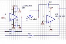
I have re-designed the modulator stage of the amplifier and substituted the MAX038 by a triangle wave generator based on two high-speed opamps (LM6172). The simulated triangle looks great and its amplitude is bigger also. If only the reality was that good!
Here is the schematic of the triangle generator. (The gain of the error signal amplifier has been risen to match the triangle amplitude)
Hello all.
I have re-designed the modulator stage of the amplifier and substituted the MAX038 by a triangle wave generator based on two high-speed opamps (LM6172). The simulated triangle looks great and its amplitude is bigger also. If only the reality was that good!
Here is the schematic of the triangle generator. (The gain of the error signal amplifier has been risen to match the triangle amplitude)
Attachments

Re: New prototype
Hi ssanmor, triangle waves turn out pretty good in real life compared to the simulation. You are much better with simulators than I am if yours can do an LM6172. I need to get some of those chips too. I have been doing class D designs using 6N137's as level shifters directly driving the IR2113. Then, the pull-up resistor provides the dead time as it fights the output capacitance of the transistor output of the 6N137. I am also considering using a couple of CD40106 / 74C14 hex Schmidt triggers and a 33pF level-shifting capacitor if I have trouble with the 6N137's. But I have done well with that high-speed optoisolator in the past and like using it
I have concluded that class D is the way to use mosfets unless for lower power, simplicity, and wholesome sound one goes with class A. Mr. Pass has got it right in that respect. For high power subwoofer amps, class D and even class AB mosfet topologies do the best. Class AB tends to operate as class A as higher frequencies are being reproduced with mosfets as output devices.
ssanmor said:Hello all.
I have re-designed the modulator stage of the amplifier and substituted the MAX038 by a triangle wave generator based on two high-speed opamps (LM6172). The simulated triangle looks great and its amplitude is bigger also. If only the reality was that good!
Here is the schematic of the triangle generator. (The gain of the error signal amplifier has been risen to match the triangle amplitude)
Hi ssanmor, triangle waves turn out pretty good in real life compared to the simulation. You are much better with simulators than I am if yours can do an LM6172. I need to get some of those chips too. I have been doing class D designs using 6N137's as level shifters directly driving the IR2113. Then, the pull-up resistor provides the dead time as it fights the output capacitance of the transistor output of the 6N137. I am also considering using a couple of CD40106 / 74C14 hex Schmidt triggers and a 33pF level-shifting capacitor if I have trouble with the 6N137's. But I have done well with that high-speed optoisolator in the past and like using it
I have concluded that class D is the way to use mosfets unless for lower power, simplicity, and wholesome sound one goes with class A. Mr. Pass has got it right in that respect. For high power subwoofer amps, class D and even class AB mosfet topologies do the best. Class AB tends to operate as class A as higher frequencies are being reproduced with mosfets as output devices.
hi subwo
If using this optocoupler take care that your circuit as a whole is fail-safe. Remember that the output of these is high if no drive signal (maybe due to failed power supply) is present at the input.
Regards
Charles
If using this optocoupler take care that your circuit as a whole is fail-safe. Remember that the output of these is high if no drive signal (maybe due to failed power supply) is present at the input.
Regards
Charles
Hi Charles, thanks for that advise. I discovered exactly what you mean. In my present design, I am counting on the protection logic of the IR2113 to prevent the outputs from turning on simultaneously. If I go with the 74C14 method, that possible problem should be sidetracked because one input will always have the inverted signal of the other.
- Status
- Not open for further replies.
- Home
- Amplifiers
- Class D
- My very first Class D pwm (switching) amplifier.