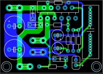
So I made my version of the LM3886 amplifier on a small 50x35mm board.
I was wondering if a groundplane for the signal part would be better than the current layout. If so, which components can be connected to this groundplane?
I have doubts about the chip pin 7, which now has a separate ground return.
Any other suggestions would be appreciated.
I was wondering if a groundplane for the signal part would be better than the current layout. If so, which components can be connected to this groundplane?
I have doubts about the chip pin 7, which now has a separate ground return.
Any other suggestions would be appreciated.
Attachments
Suggested reading: Taming the LM3886 Chip Amplifier
Not bad for a first try. I suggest using a ground plane and turning the VCC, VEE, and OUT routes into pours rather than traces. You might as well minimize the inductance there. I also suggest using a better decoupling network. You can read more on my Taming the LM3886 page linked to above.
~Tom
Not bad for a first try. I suggest using a ground plane and turning the VCC, VEE, and OUT routes into pours rather than traces. You might as well minimize the inductance there. I also suggest using a better decoupling network. You can read more on my Taming the LM3886 page linked to above.
~Tom
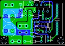
So I started with the pours for supply lines and output.
Should the power ground also be a groundplane, or is it ok as is?
Should the power ground also be a groundplane, or is it ok as is?
Attachments
Last edited:
Not bad. I still suggest a ground plane. At the very least, turn the left half of the board into a plane. You'll get better performance with a full ground plane, though. For actual data, see this thread: http://www.diyaudio.com/forums/chip-amps/252436-lm3886-pcb-vs-point-point-data-3.html#post3846783
~Tom
~Tom
Not bad. I still suggest a ground plane. At the very least, turn the left half of the board into a plane. You'll get better performance with a full ground plane, though. For actual data, see this thread: http://www.diyaudio.com/forums/chip-amps/252436-lm3886-pcb-vs-point-point-data-3.html#post3846783
~Tom
Tom,
Thanks for your input. I came up with 2 groundplanes, 1 for power / 1 for signal.
Pin 7 of the chip is now connected to the signal ground, is this ok?
Attachments
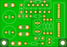
I see 4 components crossing cuts in the ground plane/s.
If I include the chip itself, that makes the count 5 !
If I include the chip itself, that makes the count 5 !
I see 4 components crossing cuts in the ground plane/s.
If I include the chip itself, that makes the count 5 !
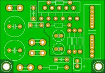
Hi AndrewT, thanks for the comments. I can learn a lot from it. Hope this is better.
Attachments
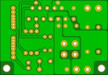
Now I see one trace joining the two upper planes.
Where do all the lower side traces pass across the cut in the upper plane?
Or do they ALL pass under that tiny linking trace?
Where do all the lower side traces pass across the cut in the upper plane?
Or do they ALL pass under that tiny linking trace?
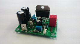
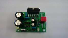
Nice! I like it. The Zobel resistor should be a power resistor, though.
You could have minimized the ground impedance a bit by rotating the supply caps and moving the Zobel closer to the IC, but what you have will likely provide the data sheet performance.
The way you joined the ground planes in Post #7 is the way you want the layout. It looks like that's where you landed on the final layout as well.
~Tom
Last edited:
Nice! I like it. The Zobel resistor should be a power resistor, though.
You could have minimized the ground impedance a bit by rotating the supply caps and moving the Zobel closer to the IC, but what you have will likely provide the data sheet performance.
The way you joined the ground planes in Post #7 is the way you want the layout. It looks like that's where you landed on the final layout as well.
~Tom
Hi, thanks for the reply.
You are right about the zobel resistor. I didn't have one available so for first test i used this 0.6W resistor. Joining the groundplanes is indeed almost the same as in post 7.
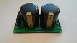
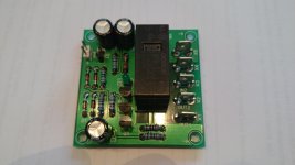
I have added a small circuit that acts as voltage regulator for the DC protection board. I can now use the V+ rails as powwersupply for the DC protection. First channel is operational and works great 🙂
Attachments

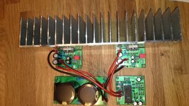
Take off those plaited wires and replace with a twisted triplet.
There are too many single wires in your assembly.
Some must be Returns for other signal Flow wires.
Close couple all signal pairs.
example. The lower right PCB has a close coupled pair of grey wires = good.
It has a close coupled pair going off screen to the right = good. but they are separated as they get closer to the amplifier.
Thay must be close coupled for the majority of the route and laid out so that they become close coupled to the traces under the PCB where they have become single wires.
The two wires exiting to the left are a disaster !
Last edited:
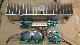
Put all the boards in a chassis now.
I found a nice potted 25V-0-25V torodial transformer that I rescued from an old sony amp.
Amp is dead silent, no hum or buzz at all.
To the right I will put a channel selection with relais later. I have made a PCB for this in the past.
I found a nice potted 25V-0-25V torodial transformer that I rescued from an old sony amp.
Amp is dead silent, no hum or buzz at all.
To the right I will put a channel selection with relais later. I have made a PCB for this in the past.
Attachments

Last edited:
- Status
- Not open for further replies.
- Home
- Amplifiers
- Chip Amps
- My take on a LM3886 layout