Now in anticipation of peoples view of ground planes and why its best to use them, I have gone through some of my document library on various aspects pf PCB design and put together a little collection of some of the documentation that I feal will help educate people on ground and power planes, de-coupling, analogue and digital ground planes, skin effect, Gerber data, EMC testing etc etc. I am in the process of trying to catalogue and store a lot of my data so please accept my appologies for the random order of some of the links. There is quite a bit of reading matter, but it is only a fraction of the stuff that you have to grasp to be a PCB designer in todays high speed, mixed digital/analoge and RF on the same board (mobile phones etc). One thing I have learned over 25 years of this is the return path (ground) is king of the board, and trying to control it with either split planes or spider leg connections causes more problems than having ground planes and letting things sort them self out. This is not getting away from the idea of signal and power grounds in amplifiers or other analogue based control designs.
Have Fun, this will keep you busy on those cold dark winter nights
http://www.elmac.co.uk/pdfs/Lord_of_the_board.pdf
Star Grounding Wars
http://www.cvel.clemson.edu/Presentation_Slides/PowerBus-Decoupling.pdf
PCB007 Quiet Power: Resonances in Power Planes
PCB007 Quiet Power: How Thin Laminates Suppress Resonances
PCB007 Do Not Perforate Planes Unnecessarily
http://www.ipblox.com/pubs/DesignCon_2011/11-TA3Paper_Weir_color.pdf
http://electrical-integrity.com/Quietpower_files/Quietpower-6.pdf
http://electrical-integrity.com/Quietpower_files/Quietpower-7.pdf
http://electrical-integrity.com/Quietpower_files/Quietpower-8.pdf
http://electrical-integrity.com/Quietpower_files/Quietpower-9.pdf
http://www.electrical-integrity.com/Paper_download_files/EPEP98_DET.pdf
Ground Pours: To Pour or Not to Pour?
http://www.goldphoenixpcb.biz/pdf/Loop_Area_Decoupling.pdf
beTheSignal - BTS-305 Battling Ferrite Superstition
http://www.speedingedge.com/PDF-Files/BTS006_What_Is_Inductance (2).pdf
MIL-STD-461: Requirements for the Control of Electromagnetic Interference Characteristics of Subsystems and Equipment - Advanced Test Equipment Rentals
http://www.sigrity.com/papers/Power Integrity Analysis December 2009.pdf
http://alicedcs.web.cern.ch/alicedcs/ElectrCoord/Documents/Gnd_gen/TIS_Grounding.pdf
http://www.nalanda.nitc.ac.in/industry/appnotes/Texas/dsp/slyt012a.pdf
http://focus.ti.com/lit/an/slyt026/slyt026.pdf
http://focus.tij.co.jp/jp/lit/an/slyt319/slyt319.pdf
http://focus.ti.com/lit/an/slyt051/slyt051.pdf
http://www.designcon.com/2010/DCPDFs/TF-MP5_Lee_Ritchey.pdf
http://focus.ti.com/lit/ml/slyp167/slyp167.pdf
http://www.e2v.com/assets/media/files/documents/broadband-data-converters/doc0999B.pdf
Printed Circuit Design & Fab Magazine Online
EMC Testing
http://www.compliance-club.com/pdf/EMCTestingPart1.pdf
http://www.compliance-club.com/pdf/EMCTestingPart2.pdf
http://www.compliance-club.com/pdf/EMCTestingPart3.pdf
http://www.compliance-club.com/pdf/EMCTestingPart4.pdf
http://www.compliance-club.com/pdf/EMCTestingPart5.pdf
http://www.compliance-club.com/pdf/EMCTestingPart6.pdf
http://www.compliance-club.com/pdf/EMCTestingPart7.pdf
MISC
http://electronica.ugr.es/~amroldan/pcb/2007/modulos/temas/ReferenceDesignators.pdf
http://www.ucamco.com/public/RS-274X_Extended_Gerber_Format_Specification_201012.pdf
http://www.downstreamtech.com/support_cam/Advisories/IPCD356_Simplified.pdf
http://pcbtalk.com/data/upload/Designing_Balanced_PCBs.pdf
http://www.pcb3d.com/uploads/PCB_Design_and_Fabrication_Process.pdf
http://www.alternatezone.com/electronics/files/PCBDesignTutorialRevA.pdf
http://www.dnu.no/arkiv1/The CAD Library of the Future.pdf
http://www.ece.unh.edu/courses/ece7...onent Zero Orientations for CAD Libraries.pdf
http://www.smtnet.com/library/files/upload/The-Universal-PCB-Design-Grid-System.pdf
Screen and stencil printing
http://www.rakon.com/Products/Public Documents/Whitepapers/PHASE NOISE IN CRYSTAL OSCILLATORS.pdf
http://www.analog.com/static/imported-files/tutorials/MT-008.pdf
Right the First Time
RF
YO3DAC\Home Page
He He
http://www.edn.com/contents/images/243231.pdf
Printed Circuit Design & Fab Magazine Online
collection of some of the documentation that I feal will help educate people on ground and power planes, de-coupling, analogue and digital ground planes, skin effect, Gerber data, EMC testing etc etc. I am in the process of trying to catalogue and store a lot of my data so please accept my appologies for the random order of some of the links. There is quite a bit of reading matter, but it is only a fraction of the stuff that you have to grasp to be a PCB designer in todays high speed, mixed digital/analoge and RF on the same board (mobile phones etc). One thing I have learned over 25 years of this is the return path (ground) is king of the board, and trying to control it with either split planes or spider leg connections causes more problems than having ground planes and letting things sort them self out. This is not getting away from the idea of signal and power grounds in amplifiers or other analogue based control designs.Have Fun, this will keep you busy on those cold dark winter nights
http://www.elmac.co.uk/pdfs/Lord_of_the_board.pdf
Star Grounding Wars
http://www.cvel.clemson.edu/Presentation_Slides/PowerBus-Decoupling.pdf
PCB007 Quiet Power: Resonances in Power Planes
PCB007 Quiet Power: How Thin Laminates Suppress Resonances
PCB007 Do Not Perforate Planes Unnecessarily
http://www.ipblox.com/pubs/DesignCon_2011/11-TA3Paper_Weir_color.pdf
http://electrical-integrity.com/Quietpower_files/Quietpower-6.pdf
http://electrical-integrity.com/Quietpower_files/Quietpower-7.pdf
http://electrical-integrity.com/Quietpower_files/Quietpower-8.pdf
http://electrical-integrity.com/Quietpower_files/Quietpower-9.pdf
http://www.electrical-integrity.com/Paper_download_files/EPEP98_DET.pdf
Ground Pours: To Pour or Not to Pour?
http://www.goldphoenixpcb.biz/pdf/Loop_Area_Decoupling.pdf
beTheSignal - BTS-305 Battling Ferrite Superstition
http://www.speedingedge.com/PDF-Files/BTS006_What_Is_Inductance (2).pdf
MIL-STD-461: Requirements for the Control of Electromagnetic Interference Characteristics of Subsystems and Equipment - Advanced Test Equipment Rentals
http://www.sigrity.com/papers/Power Integrity Analysis December 2009.pdf
http://alicedcs.web.cern.ch/alicedcs/ElectrCoord/Documents/Gnd_gen/TIS_Grounding.pdf
http://www.nalanda.nitc.ac.in/industry/appnotes/Texas/dsp/slyt012a.pdf
http://focus.ti.com/lit/an/slyt026/slyt026.pdf
http://focus.tij.co.jp/jp/lit/an/slyt319/slyt319.pdf
http://focus.ti.com/lit/an/slyt051/slyt051.pdf
http://www.designcon.com/2010/DCPDFs/TF-MP5_Lee_Ritchey.pdf
http://focus.ti.com/lit/ml/slyp167/slyp167.pdf
http://www.e2v.com/assets/media/files/documents/broadband-data-converters/doc0999B.pdf
Printed Circuit Design & Fab Magazine Online
EMC Testing
http://www.compliance-club.com/pdf/EMCTestingPart1.pdf
http://www.compliance-club.com/pdf/EMCTestingPart2.pdf
http://www.compliance-club.com/pdf/EMCTestingPart3.pdf
http://www.compliance-club.com/pdf/EMCTestingPart4.pdf
http://www.compliance-club.com/pdf/EMCTestingPart5.pdf
http://www.compliance-club.com/pdf/EMCTestingPart6.pdf
http://www.compliance-club.com/pdf/EMCTestingPart7.pdf
MISC
http://electronica.ugr.es/~amroldan/pcb/2007/modulos/temas/ReferenceDesignators.pdf
http://www.ucamco.com/public/RS-274X_Extended_Gerber_Format_Specification_201012.pdf
http://www.downstreamtech.com/support_cam/Advisories/IPCD356_Simplified.pdf
http://pcbtalk.com/data/upload/Designing_Balanced_PCBs.pdf
http://www.pcb3d.com/uploads/PCB_Design_and_Fabrication_Process.pdf
http://www.alternatezone.com/electronics/files/PCBDesignTutorialRevA.pdf
http://www.dnu.no/arkiv1/The CAD Library of the Future.pdf
http://www.ece.unh.edu/courses/ece7...onent Zero Orientations for CAD Libraries.pdf
http://www.smtnet.com/library/files/upload/The-Universal-PCB-Design-Grid-System.pdf
Screen and stencil printing
http://www.rakon.com/Products/Public Documents/Whitepapers/PHASE NOISE IN CRYSTAL OSCILLATORS.pdf
http://www.analog.com/static/imported-files/tutorials/MT-008.pdf
Right the First Time
RF
YO3DAC\Home Page
He He
http://www.edn.com/contents/images/243231.pdf
Printed Circuit Design & Fab Magazine Online
You are more likley these days (and in the past) to cause more problems by trying to control the return path. The first thing is to change the way you think about how signals propogate on PCB's (as well as other media), best explained by this link:
Printed Circuit Design & Fab Magazine Online
" This new worldview of current propagation is based on the return current being just as important as the signal current. "
Nothing new here, one off Kirchoffs' laws
True Guido, but how many people look at signal transmission in that way, when they are doing boards, or connecting any system together? most people still view it as the lightbulb illustration from the Link, especially if you are not involved with PCB layout, EMC, Signal Integrity and Power Delivery System Integrity every day of your life.
At the end of the day I'm just putting up a selection of information from my collection, I believe could be informative and helpfull to those who want to learn PCB design in a bit more depth.
At the end of the day I'm just putting up a selection of information from my collection, I believe could be informative and helpfull to those who want to learn PCB design in a bit more depth.
True Guido, but how many people look at signal transmission in that way, when they are doing boards, or connecting any system together? most people still view it as the lightbulb illustration from the Link, especially if you are not involved with PCB layout, EMC, Signal Integrity and Power Delivery System Integrity every day of your life.
At the end of the day I'm just putting up a selection of information from my collection, I believe could be informative and helpfull to those who want to learn PCB design in a bit more depth.
Yes, you are right. What irritated me was that the author of the link acts as if he has invented something new.....
cheers
OK,
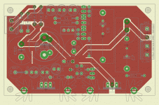
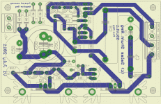
I finally settled down for the following layout and design.
It is still quite compact (although not as much as I wanted originally, but I had to make compromises)
I decided to keep a combination of Star grounding and Ground Plane (star ground to isolate the ground from the rectified current and avoid ground loops, and plane to provide some RFI protection)
The argument/analogy with the 3 antenna made me think a lot but I finally decided to go for it anyway with the following reasons:
- in the case of 2.4GHz GSM antennas, the use of multiple antennas does not intrinsically increase the radiation, but rather makes it omnidirectionnal. My opinion is that using 3 antennas will not radiate more than one if there is the same power at the input.
- This is a shunt Reg working at audio frequency, not a high frequency switching circuit, so it doesn't radiate in the first place.. I guess I don't need to worry of RFI anyway
- ... and this is DIY after all.. who cares if my design does not pass the EMC tests!
Unless I receive any further comment on the design by then, I'll send the files to the board house this week end (if I succeed in making the Gerber Files)
I want to thank all of you for the very usefull and informative comments on the design and how to improve it. I guess I learned a lot from this thread on designing PCBs and RFI theory !
Fred
Attachments
- Status
- This old topic is closed. If you want to reopen this topic, contact a moderator using the "Report Post" button.