Hi Terry,
First, I should correct myself, I neglected that each side of the first pair (“non-inverting input” or “base”) of the transistors (of both stages) presents one current path, so there are 7 current paths and the similar currents seemingly run through the current source (voltage reference) circuitry, so 9 paths in total. Since there are no emitter resistors, not shown at least… yes, it outcomes to about 3mA (or should I say +/-3mA). Which for 1k is not bad at all if you consider it is the diamond transistor. Higher current, if it would be possible, probably would bring some improvement, but, as I said, almost certainly, it is not a major issue here. For this purpose, some other issues like maximum supply voltage of the OPA660 appear as more important.
Pedja
Considering the bias current the answer is no, 5 arrays of AD844 share 6.5mA. Maximum supply voltage is however healthy +/-18V.tbla said:would the ad844 be a better choice........?
Also, note that the circuits are a bit different.
Pedja
Pedja said:Hi Terry,
First, I should correct myself, I neglected that each side of the first pair (“non-inverting input” or “base”) of the transistors (of both stages) presents one current path, so there are 7 current paths and the similar currents seemingly run through the current source (voltage reference) circuitry, so 9 paths in total. Since there are no emitter resistors, not shown at least… yes, it outcomes to about 3mA (or should I say +/-3mA). Which for 1k is not bad at all if you consider it is the diamond transistor. Higher current, if it would be possible, probably would bring some improvement, but, as I said, almost certainly, it is not a major issue here. For this purpose, some other issues like maximum supply voltage of the OPA660 appear as more important.
Pedja
WRT 3mA bias current for +-2mA/1~2k OP Z DAC, I can only
suggest you do some listening tests and measurements with
AP or the like. I've done both and 3mA aint enough.
Cheers,
Terry
Tbla, Terry, others,
Lately I came across the info about the other two chips which can be used this way. These are Maxim MAX435/436. To figure the way they could be used, much better than their datasheet is to check this Maxim’s application note. Supply voltage is unfortunately again limited to +/-6V. There are SPICE models, but very reduced so they are usable in a very limited way. But were enough to confirm that the chips can work for this purpose.
Pedja
Just to clarify: have you done it with the diamond transistor (complementary circuit!)? If you did, then you are right. If you did not... the circuit is known as one with extremely good driving capabilities.Terry Demol said:WRT 3mA bias current for +-2mA/1~2k OP Z DAC, I can only
suggest you do some listening tests and measurements with
AP or the like. I've done both and 3mA aint enough.
Pedja
Thanks a lot for that answers.
Yes,I guess I'm expecting too much from it (ultimate is good word for what I want).
I will surely try Rudolf's super pair.
Bartek
The OPA660 is a good idea from the outset but when you really think it through it has too many limitations for really
ultimate 0 FB I-V conversion
Yes,I guess I'm expecting too much from it (ultimate is good word for what I want).
I will surely try Rudolf's super pair.
Bartek
Pedja said:
Just to clarify: have you done it with the diamond transistor (complementary circuit!)? If you did, then you are right. If you did not... the circuit is known as one with extremely good driving capabilities.
Pedja
Pedja, all 0 FB I-V implementations we have done are discrete.
Whether they are discrete or chip is irrelevant WRT basic
non lineartity of grounded base stage due to lack of quiescent
current and low DAC OP Z (around 1k).
Cheers,
Terry
Terry, I did not say it has to be monolithic. I asked you did you try that circuit, be it monolithic or discrete. Mainly it is indeed irrelevant if it is monolithic or discrete but it is not irrelevant what circuit is used. So, according to this, you can not speak like “grounded base stages need this or that bias current to accept this or that DAC current of this or that output impedance”. Just for the info, I am aware of the fact for the most circuits posted here by Rudolf and Jocko it is probably best to run them at 5-10mA.
So, once more, my remark applies to the circuit used in the OPA660. Built something like that? Varied the current? How much it improved raising the current from 3mA to, say, 6mA? Have you found some other parameters more important? Was the 3mA major issue? Thanks.
Pedja
So, once more, my remark applies to the circuit used in the OPA660. Built something like that? Varied the current? How much it improved raising the current from 3mA to, say, 6mA? Have you found some other parameters more important? Was the 3mA major issue? Thanks.
Pedja
Pedja said:Terry, I did not say it has to be monolithic. I asked you did you try that circuit, be it monolithic or discrete. Mainly it is indeed irrelevant if it is monolithic or discrete but it is not irrelevant what circuit is used. So, according to this, you can not speak like “grounded base stages need this or that bias current to accept this or that DAC current of this or that output impedance”. Just for the info, I am aware of the fact for the most circuits posted here by Rudolf and Jocko it is probably best to run them at 5-10mA.
So, once more, my remark applies to the circuit used in the OPA660. Built something like that? Varied the current? How much it improved raising the current from 3mA to, say, 6mA? Have you found some other parameters more important? Was the 3mA major issue? Thanks.
Pedja
Hi Pedja,
Yes we did try a complimentary GBS. It was fed into cascodes
and not current mirrors as in the 660, however a well designed
cascode will be superior than mirrors in linearity and noise
performance in this application.
WRT bias current I think a good way to get a feel for
it is to get access to a HQ measuring set such as AP and
plug away on various circuits with various loads and V swing.
It really does show you where all the non linearities lie.
I sat there for a month a while back with AP and just
breadboarded every circuit I could think of and measured
distortion vs loads vs currents vs swing with BJT's MOS
and JFETs. The results were very interesting to say the least.
I won't say any more except that I feel it is possible to make
a discrete 0 FB I-V with 120dB dynamic range.
Cheers,
Terry
Discrete!
Hi Terry,
Am I reading this right? -0- FB 120db dynamic range?
Please tell me more........... I want to use something like that in my TEAC!
Can you shear the schematic with us? Please? Or is it allready on this forum?
Thanks.
Audiofanatic 😉
Hi Terry,
I won't say any more except that I feel it is possible to make a discrete 0 FB I-V with 120dB dynamic range
Am I reading this right? -0- FB 120db dynamic range?
Please tell me more........... I want to use something like that in my TEAC!
Can you shear the schematic with us? Please? Or is it allready on this forum?
Thanks.
Audiofanatic 😉
Terry,
I spent some time spicing common base circuits and because of that I however feel like I do have certain feel about what and how it should be done. Among the other things, I came across the conclusion that the very similar (principally the same) circuit to that one used in the OPA660, with a few changes and if runs at higher voltages, with 4mA p-p output current of 1k output Z DAC, can have THD below 0.001% (none harmonic above -100dB). All that with the input stage (“emitter”) biased at 4-4.5mA. Higher current brings nothing here! Trust me, I know what I am talking about. I checked this today again. I did not breadboarded it yet and yes, when I’ll do that I’ll measure it, it is understood (and btw I certainly don’t need AP for this).
Pedja
Terry Demol said:
WRT bias current I think a good way to get a feel for
it is to get access to a HQ measuring set such as AP and
plug away on various circuits with various loads and V swing.
It really does show you where all the non linearities lie.
I sat there for a month a while back with AP and just
breadboarded every circuit I could think of and measured
distortion vs loads vs currents vs swing with BJT's MOS
and JFETs. The results were very interesting to say the least.
I won't say any more except that I feel it is possible to make
a discrete 0 FB I-V with 120dB dynamic range.
Cheers,
Terry
Lacking access to this kind of measurement systems (can borrow a scope with FFT module, but that will not really suffice), I derived operating currents and voltages using spice modeling, datasheet info, "good practises" and common sense.
Terry, I would be very interested for any hints, attention points to optimize and/or improve the latest I/V incarnation I use, with folded cascode and super-pair.
The cascode on the current sink "seeing" the output voltage swing turned out very important, BTW, Spice gave same thd numbers, with or without !
I guess it's common sense choosing the Riv as small as one really needs.
I never tried the chip solution like OPA660 because first it can't be used directly with the TDA1543.
It uses a diffent approach as well as you state, mirrors in stead of (folded) cascodes.
Also the current draw on both rails are modulated by the dac current output (input), whereas the discrete circuits without mirrors have nearly constant current draw, which is quite an important difference IMHO. Even with constant current draw, one can still hear the type of capacitors used on rails, so it "sounds" like everything matters...
Peter Daniel has done some very interesting tests in this area.
Pedja said:Terry,
I spent some time spicing common base circuits and because of that I however feel like I do have certain feel about what and how it should be done. Among the other things, I came across the conclusion that the very similar (principally the same) circuit to that one used in the OPA660, with a few changes and if runs at higher voltages, with 4mA p-p output current of 1k output Z DAC, can have THD below 0.001% (none harmonic above -100dB). All that with the input stage (“emitter”) biased at 4-4.5mA. Higher current brings nothing here! Trust me, I know what I am talking about. I checked this today again. I did not breadboarded it yet and yes, when I’ll do that I’ll measure it, it is understood (and btw I certainly don’t need AP for this).
Pedja
Hi Pedja,
Interesting, my real world measurements on AP1 don't
come anywhere near this, and that is without the current
mirrors which will have their own non linearities.
By virtue of the fact that your simulator shows no improvement in
linearity with increase in current is a worry, something is amiss
here? Basic rule of BJT linearity, emmiter Z = 0.026/current. More
current = better linearity within the limits of other conflicting
parameters such as noise and non linear HFE. My measurements
reflected this exactly.
I wish I had an OPA660 around so I could measure it.
Cheers,
Terry
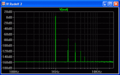
Below are the simulated harmonic distortion graphs of three common base I/V stages. Source output current is 4mA p-p, source output Z is 1kOhm, I/V resistor is 1.5kOhm.
Rudolf 1 is the single transistor between the current source and current sink. The circuit was firstly posted by Jocko and later posted by Rudolf about year ago. The circuit is supplied by +/-18V and signal transistor runs at 7mA.
Rudolf 2 is a few months old Rudolf’s circuit with folded cascode (not super pair). The first (input) transistor runs at 11mA.
Third is the one circuit very similar to that one used in the OPA660. It is supplied by +/-24V and the first stage runs at somewhat less than 4.5mA. However, the circuit exactly used in the OPA660 can not show this performance regardless of the used voltage and current. Or at least I have not found the way to do that. Judging on the OPA660 model provided by BurrBrown, with the same 1kOhm Out Z, 4mA p-p current source and used as common base stage with 1.5kOhm I/V resistor, it will have about 0.06% THD (mainly third harmonic).
Simulations are done using BC547C/557C models by Philips.
For possible better insight, the same circuits with the same operating points simulated using 2N4401/4403 models by Fairchild.
The graphs are not supposed to claim anything about the sonics. Especially I do not have an intention to claim that the last shown circuit will work better than the first two. Btw, even better numbers are achievable using a complementary feedback pair.
Pedja
Rudolf 1 is the single transistor between the current source and current sink. The circuit was firstly posted by Jocko and later posted by Rudolf about year ago. The circuit is supplied by +/-18V and signal transistor runs at 7mA.
Rudolf 2 is a few months old Rudolf’s circuit with folded cascode (not super pair). The first (input) transistor runs at 11mA.
Third is the one circuit very similar to that one used in the OPA660. It is supplied by +/-24V and the first stage runs at somewhat less than 4.5mA. However, the circuit exactly used in the OPA660 can not show this performance regardless of the used voltage and current. Or at least I have not found the way to do that. Judging on the OPA660 model provided by BurrBrown, with the same 1kOhm Out Z, 4mA p-p current source and used as common base stage with 1.5kOhm I/V resistor, it will have about 0.06% THD (mainly third harmonic).
Simulations are done using BC547C/557C models by Philips.
An externally hosted image should be here but it was not working when we last tested it.
For possible better insight, the same circuits with the same operating points simulated using 2N4401/4403 models by Fairchild.
An externally hosted image should be here but it was not working when we last tested it.
The graphs are not supposed to claim anything about the sonics. Especially I do not have an intention to claim that the last shown circuit will work better than the first two. Btw, even better numbers are achievable using a complementary feedback pair.
Pedja
Pedja said:Below are the simulated harmonic distortion graphs of three common base I/V stages. Source output current is 4mA p-p, source output Z is 1kOhm, I/V resistor is 1.5kOhm.
Thanks for the graphs Pedja. Very interesting results.
Yes, this one is SE, non cascoded and shows a fair degree of
Rudolf 1 is the single transistor between the current source and current sink. The circuit was firstly posted by Jocko and later posted by Rudolf about year ago. The circuit is supplied by +/-18V and signal transistor runs at 7mA.
non linearity
This one is a bit perplexing. I don't understand why H2 has
Rudolf 2 is a few months old Rudolf’s circuit with folded cascode (not super pair). The first (input) transistor runs at 11mA.
been attenuated compared H3. I would have thought the
cascode AND higher current (11mA) would lower all harmonics.
On this premise H3 should be lower than -80dB. Maybe the
cascode is non ideal, but looking at specs of 2SA1085 all looks
good up to 10mA (HFE linearity).
I am looking at the OP current source as a possible culprit.
If you have time, try cascoding this.
I'm sure the super pair will improve on these measurements,
but Rudolf, maybe the OP current source should also be
a super pair to make it more ideal. Food for thought.
Does it include current mirrors or complimentary cascodes?
Third is the one circuit very similar to that one used in the OPA660. It is supplied by +/-24V and the first stage runs at somewhat less than 4.5mA.
I am surprised it simulates so well. If you can explain circuit details
next time I have AP1, I will knock one up and measure it.
This is more the level I would expect in real life if not a little
However, the circuit exactly used in the OPA660 can not show this performance regardless of the used voltage and current. Or at least I have not found the way to do that. Judging on the OPA660 model provided by BurrBrown, with the same 1kOhm Out Z, 4mA p-p current source and used as common base stage with 1.5kOhm I/V resistor, it will have about 0.06% THD (mainly third harmonic).
better.
WRT CFP, yes of course, I would expect at least 20dB
The graphs are not supposed to claim anything about the sonics. Especially I do not have an intention to claim that the last shown circuit will work better than the first two. Btw, even better numbers are achievable using a complementary feedback pair.
Pedja
improvement.
Also I would try simulations at 10kHz. When I did
measurements, this often really broke a particular designs
back. Where as many designs measured well at 1k some had
20dB or worse results at 10kHz. I strived for almost flat
measurements from 1kHz -> 10kHz. I think this is where
designs like super pair will excel.
So what have we learned? I'm not sure, however I would
certainly like to run simulation parallel to physical measurements
next time I have AP1 in my hands, this will answer a lot of
questions.
What software are you using, where can I get it?
Good post, thanks for the effort. 🙂
PS All this typing is chewing up my DAC building time🙁
Cheers,
Terry
Terry, I have looked again through this and take my apologies, the first transistor was running at 11mA but cascoding device on 3mA. I raised this to 8mA and the result is below (so consider this instead of the second graph in the first string above). Of course, all this puts higher demands on the (upper) current source which should then provide 19mA. As about this current source, I tried earlier two ways to improve it in the basic circuit and both showed lower harmonic distortion but in this regard it seems not to be that important for the cascoded circuit.Terry Demol said:This one is a bit perplexing. I don't understand why H2 has
been attenuated compared H3. I would have thought the
cascode AND higher current (11mA) would lower all harmonics.
On this premise H3 should be lower than -80dB. Maybe the
cascode is non ideal, but looking at specs of 2SA1085 all looks
good up to 10mA (HFE linearity).
I am looking at the OP current source as a possible culprit.
If you have time, try cascoding this.
Just drop me an address on react_71@yahoo.com .Does it include current mirrors or complimentary cascodes?
I am surprised it simulates so well. If you can explain circuit details
next time I have AP1, I will knock one up and measure it.
Linear Technology SwitcherCAD, free, fully working, serious SPICE program, downloadable from here:So what have we learned? I'm not sure, however I would
certainly like to run simulation parallel to physical measurements
next time I have AP1 in my hands, this will answer a lot of
questions.
What software are you using, where can I get it?
http://www.linear.com/software/
Pedja
Attachments
Pedja said:
Terry, I have looked again through this and take my apologies, the first transistor was running at 11mA but cascoding device on 3mA. I raised this to 8mA and the result is below (so consider this instead of the second graph in the first string above). Of course, all this puts higher demands on the (upper) current source which should then provide 19mA. As about this current source, I tried earlier two ways to improve it in the basic circuit and both showed lower harmonic distortion but in this regard it seems not to be that important for the cascoded circuit.
Thanks for the update Pedja,
Looking at these results, seems cascode can be improved
slightly but thats almost another thread. I am wondering whether
SwitcherCAD takes into account noise generated by current
sources. The noise floors you are getting appear to be very low,
almost too low?
Current source noise has not been discussed much here.
Every current source has a "noise gain" that develops into load R.
For example a current source with a 100R current generating R
will have a noise gain of 15 WRT 1k5 load R.
So the 1.3nV/rt Hz of 100R will end up 19.5nV/rt Hz at OP.
If the ref. BJT has say 1.5nV/rt Hz then it will be 22.5nV/rt Hz at
OP. All these noise sources will add RMS. So as you can see when
current goes up, noise can be difficult to manage. Also WRT
current mirrors, they will have much larger noise gain than a
conventional current source, another reason I don't like 660
or anything that uses mirrors, unless they can be degenerated
to lower the noise gain.
I have used degeneration of current mirrors (with 330R)
successfully in microphone preamps to lower noise and it worked
well. Also makes mirror more linear but the downside is induced
voltage swing (however small).
Another aspect to consider is any other current source
components' audible effects, such as electrolytic caps for example,
will be subject to this noise gain.
Years ago we found various components in current sources
tend to be more audible than would be imagined. Often we
treat a current source as a "function block" which has little
audible effect, however once you consider the noise gain into
OP load, things make a bit more sense.
Thanks for SwitcherCAD link I will download it and simulate some
circuits I have already measured, see how they compare. I will
also be keen to simulate some of the many I-V ideas I haven't
even had time to try.
Cheers,
Terry
Hi Terry,
Interesting notice about the current source noise.
Re the noise floor on the graphs above, actually, none windowing was applied in the FFT, and Blackman and Hanning will bring improvement of further 20-30dB. Since in this case the noise floor looks a bit nervous, for the sake of the visual elegancy I left the “raw” FFT’s nice flat line. I do not take this too serious because many noise sources that will appear in the real world are certainly not modeled at all.
Pedja
Pedja said:Hi Terry,
Interesting notice about the current source noise.
Re the noise floor on the graphs above, actually, none windowing was applied in the FFT, and Blackman and Hanning will bring improvement of further 20-30dB. Since in this case the noise floor looks a bit nervous, for the sake of the visual elegancy I left the “raw” FFT’s nice flat line. I do not take this too serious because many noise sources that will appear in the real world are certainly not modeled at all.
Pedja
Exactly. However, the OP noise can be calculated if all the devices
noises are known, assuming power supply is not limiting.
It's just a matter of understanding what all the noise
generating mechanisms are. A current source is not just
a current source.
Cheers,
Terry
- Status
- Not open for further replies.
- Home
- Source & Line
- Digital Source
- My OPA 660 I-V stage for TDA 1541A