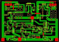
What I would now is print the layout to scale and see how it looks.
Some of the large pads (if it were me) have a bit to much "hole". I'd make the hole smaller while keeping the same pad size. When you come to solder you want the component legs to be as near to the copper as possible. If you are drilling by hand then I find 1mm or even 0.8mm holes a good size for the PCB. The hole in the pad is just needed to start the PCB.
Some of the large pads (if it were me) have a bit to much "hole". I'd make the hole smaller while keeping the same pad size. When you come to solder you want the component legs to be as near to the copper as possible. If you are drilling by hand then I find 1mm or even 0.8mm holes a good size for the PCB. The hole in the pad is just needed to start the PCB.
Big holes on the pads are because of my software. I can't change the hole diameter without changing the the pad size. I also see that the holes are too big. I use ExpressPCB - any idea how to fix that?
Today was the actual build!
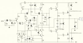
Yes today was the actual build but schematic was different. After an not very successful build with the EF buffered VAS I decided to give a try a cascoded VAS. Also I moved the trimmer for the DC offset and OS is Quasi now. So I build the schematic on the picture on veroboard , powered up and listened. All connections from the board to the drivers and output transistors was with long wires and incredibly there was no any hum and buzz. Sound was not bad but I tested one channel only and dont have full impressions.
Now several questions : I will use this schematic with +/- 50 V supply. BD139/140 cant be used so with what to substitute them? I dont like MJE340/350!
Will one pair IRFP260N be enough to use safe with 4R load?
Any other comments on the schematic are welcome.
Best Regards!
P.S. Here in Bulgaria we have a really bad snow now. I wasnt seen something like this from years!
PS2: Oops I attached a wrong picture! Actually the only difference with real schematic is that there is no 100R resistors in the driver bases also 10pF in NFB is not absolutely necessary no problem without it - test was without.
Attachments
Last edited:
For real world domestic use I think a single pair is OK, even on -/+50 volts. There is a world of difference in sustained high power testing into 4 or 8 ohm.
If you really want to drive it as a lab amp into 4Ω or 8Ω at maximum output then multiple pairs are advised.
Single pairs are often sonically better too... the capacitive loading is that much less.
Drivers... hmmm depends what you can get. How about the 2SA1209/2SC2911 or second choice, the 2SA1668/2SC4382.
Just a typo on C10. T'Other way up 🙂
Output inductor ? You never know what someone might hang on the end of it.
Thanks for the comment , Mooly!
Yes C10 drawn in wrong way. I can get 2SC4793 and his brother are they suitable for VAS and drivers? Output inductor is also good to have it but how to make it?
Is there something in the schematic that can be made better or is OK like I make it?
I'm asking because still testing the amp and if someone can tell me what can be made better will test and post the result.
Best regards!
The 2SC4793/2SA1837 should be good.
Output inductors are pretty non critical in absolute terms.
This is quoting D Self... "air cored... around 6uH... 20turns of 1.5mm copper wire... around 1 inch diameter". You can also add a 10 ohm carbon 1 watt resistor across the coil for damping.
It's very non critical. It goes after R25/C13 of course.
You could also try (on listening tests) adding small series output resistor of around 0.1 to 0.33 ohms. By raising the output impedance the speaker impedance comes into play modifying the overall response. Some like it, some don't. You must listen to it carefully and critically.
Edit... picture of output inductors from my amp. I wound these round an old electro cap as a former.
http://www.diyaudio.com/forums/solid-state/191449-output-relays-14.html#post2660474
Last edited:
Second Attempt!
After listening tests I increased the driver stage current to near 50mA. It gives a much better detail and HF response also added the new values for the higher supply voltage , output coil , gate protection zeners and I made better more understandable drawing.
So any comments?
Regards!
PS: Why when I put an emoticon in the text after submitting post it disappears? Is this happening only with me?
Attachments
Last edited:
😀 typed out and and😀  as emoticons.
The increased driver current will certainly make for better hf perfomance.
It would be an interesting experiment to compare the HEXFET's with Laterals sonically in an amplifier of this topology.
Edit...... emoticons.... yep, just you 😛
as emoticons.The increased driver current will certainly make for better hf perfomance.
It would be an interesting experiment to compare the HEXFET's with Laterals sonically in an amplifier of this topology.
Edit...... emoticons.... yep, just you 😛
🙂 another icons test.
Will be interesting for me too to compare V-FETs with L-FETs .
What browser do you use? I use Firefox latest version.
Edit.....now have emoticons but not all one is missing.
another icons test.Will be interesting for me too to compare V-FETs with L-FETs .
What browser do you use? I use Firefox latest version.
Edit.....now have emoticons but not all one is missing.


Moving forward!
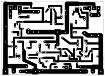
Here is my first attempt to make a PCB. I have question too what is better -to put the output coil on the output terminals of the amp or directly on the PCB?
You can see that putting it on PCB will be difficult right now.
Any advises will be much helpful. Attaching the schematic and PCB.
Here is my first attempt to make a PCB. I have question too what is better -to put the output coil on the output terminals of the amp or directly on the PCB?
You can see that putting it on PCB will be difficult right now.
Any advises will be much helpful. Attaching the schematic and PCB.
Attachments
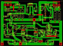
That looks a very good first attempt to me. Is it done with Diptrace ?
The only advice I can think of on the PCB is to make pads as large as possible. They look big on here, they won't in reality. For visual neatness I try and take angles and sloping lines out where possible... I'm not trying to find fault 🙂 it's a great first attempt.
I do mine on an ordinary inkjet printer with transparency film and a UV box. Make sure you turn off the silk screen (not the first time I been caught out there) and that you have the image printed "correct" or "mirrored" depending how you work.
R25 and C13 are the important ones to get on the PCB which you have, The coil can be anywhere between PCB and output terminals.
Well it is first attempt for this schematic not first PCB but I do made only 2-3 PCB's so I'm not an expert 😀
Will try to "polish" it a bit and make it to catch the eye 😉 and will enlarge the pads.
Will make it with the toner transfer method because I have a laser printer.
I use a ExpressPCB - it is not very good software but simple enough for a beginner like me. I tried other software including DipTrace but seems to be too complex for me. 😛😕😉
Thanks for the comment!
Regards!
Last edited:
Second attempt!
Here it is - larger pads and smooth lines.
It is becoming better isn't it?
More advises are welcome!
Something else - my browser put the wrong emoticons in my previous post 😡 so I'm sorry for that 😱 leaving Firefox forever moving to Crome.
Here it is - larger pads and smooth lines.
It is becoming better isn't it?
More advises are welcome!
Something else - my browser put the wrong emoticons in my previous post 😡 so I'm sorry for that 😱 leaving Firefox forever moving to Crome.
Attachments
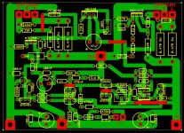
It's really good 🙂
The 2N5401 and 2N5551 at the bottom. Could you rotate them 180 degrees to eliminate links ? Or have you done it that way thinking of thermal contact between them. In practice not an issue I think 🙂
Print it all out to scale and see how the components fit, caps in particular. The holes in the large pads including FET's. See what you think when printed. I tend to make the large holes around 1mm, just enough to locate the drill bit. It won't look as good on screen but much much better to work with when it's copper. Otherwise you are "filling" the hole with solder.
Yes you are right I made them like that for a thermal contact but it is really no big deal - offset was very stable in the test build and there was no thermal contact so I will rotate them to eliminate the links. Also I changed the tracks a bit in 2-3 positions - it is better I think 🙂.
About the holes....this is one of the drawbacks of my software it can't be adjusted but I think it is time to get a better software. Yesterday I downloaded and installed DipTrace - it is very complicated compared to current one but will start learnig it and will try to redraw it. A question about DipTrace - do I need to
draw a schematic first and then to create PCB from it or directly to draw a board?
See how it looks now:
Last edited:
Sorry for double posting but time for editing expired just before submitting.
There is way to create a custom pad sizes actually but I just noticed it.
No cure for human stupidity...

I also forgot to put the compensation capacitor in the NFB so it is corrected.
See how it looks now:
There is way to create a custom pad sizes actually but I just noticed it.
No cure for human stupidity...
I also forgot to put the compensation capacitor in the NFB so it is corrected.
See how it looks now:
Attachments
Your transistor choices are a little misguided. For vas the BD139 will be far superior to ksc2690. While cascoding does reduce the miller effect it doesnt eliminate it so your choice will have higher high frequency distortion. Ksc2690 has double or more the cob of BD139. Ideally in a vas with cascode you should look at the lowest cob and high beta transistor, the high beta will reduce vas output impedance and lower THD due to vas loading effects. You could even use a single darlington transistor for this position for optimum performance.
Your cascode transistor should also be a low cob type but here the most important is to have a very high early voltage, in that respect ksc2690 or 2sa1837 is not too bad but there are other types better suited and with lower cob.
Simulations dont accurately reflect the mechanisms at work here but you could confer via actual measurements.
- Status
- Not open for further replies.
- Home
- Amplifiers
- Solid State
- My new design or updated old one