Hi guys,
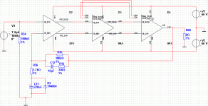
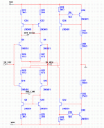
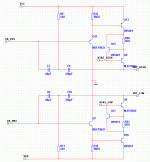
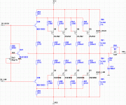
I'm building a Mosfet amplifier based on a selfmade circuit design (mostly based on techniques and building blocks learned from Randy Slone's book "High Power Audio Amplifier Construction Manual"), as can be seen in the attached schematics (I divided the schematics into blocks to make it more readable. The three triangular symbols contains respectively the input stage, voltage amplification stage and output stage, whose schematics will be posted in the next posts).
The circuit as it is seen in the attachments works great in Electronics Workbench, and simulation results are quite pleasing. I have now hooked it up on breadboard for real life testing, and some problems have occurred.
as long as I don't connect a speaker (or any load) it seems to be working fine, it reproduces the applied sine wave at various frequencies very nicely, and with quite low distortion (measured 0,4% at 1 kHz).
when I connect a speaker (8 Ohms) it starts acting weird. Upon power up, a lot of strange noises are heard in the speaker and the lower output device conducts approx 1-2 amps of current. After a few seconds the noise is silenced, and I'm attempting to play music. it is possible to recognize which song is played, but not more to it than that. The distortion is massive, and the sound is very grainy, somewhat like listening to a very badly tuned radio, to put a word on it.
The problem seems to have something to do with the biasing of the output devices. The sound seems to disappear completely on low volumes, and I measure -0,43 Volts on both the collector and emitter of the amplified diode transistor (Q22 in the output stage).
The test setup differs from the schematics by the following:
- Rail voltages are +/- 32 Volts (maximum available from my lab supply)
- MJ15032/MJ15033 transistors replaced with 2SC2073/2SA940 (also tested with 2SD669/2SB649, didn't help the problems)
- Only one pair of output devices
- the pot used for adjusting the bias current is rated 20K instead of 1K
- Resistors R54 and R55 in the output stage are 91 Ohms
- Resistors R56 and R57 in the output stage are 10 Ohms (the ratio between these and the R54/R55 should be 10).
Any suggestions? Is there anything wrong with the design, or are the problems caused by the changes made to the test setup?
Attachments
Without looking at your schematics - if it simulates OK then there's good reason to think that it'll work OK if you build it OK. This is one of the reasons I like to go from schematic to PCB rather than breadboard or veroboard.
If you can possibly get somebody else to check your connections on the breadboard they may notice a mistake in assembly. It can be very difficult to debug something you have built wrong because of your involvement with it. Otherwise go through it connection by connection with the greatest concentration and check also that the components are correct and of the correct value.
w
thanks for replying. Yes, I might agree that the breadboard way hooking up a circuit itself is far from optimum for a sophisticated circuit like this. Initially, I hooked up the Input and VAS stage only, leaving the output stage out of the picture. After several test runs and correcting errors, I made it run smoothly, however with somewhat high THD (approx. 1.5% at 1 kHz). So I'm 99,5% confident that the wiring is correct and in accordance with the schematics 🙂
One note on the EWB simulations: EWB didn't come with models of the 2SK1058/2SJ162, so I had to create models based on SPICE model data found in a post here on this forum. I am still not 100% sure that the transistor models I use for these in the sims are correct...
but thanks for the advice, maybe I'll go ahead and put the thing on a PCB before I give up 🙂
You could try these
*SRC=2SK1058;MSK1058;MOSFETs N;Power >100V;160V 7A
*SYM=POWMOSN
.SUBCKT MSK1058 10 20 40
* TERMINALS: D G S
* Hitachi 160 Volt 7 Amp .171 ohm N-Channel Power MOSFET 08-06-1993
M1 1 2 3 3 DMOS L=1U W=1U
RD 100 1 80.4M
RS 30 3 5.28M
RG 20 2 21.4
CGS 2 3 410P
EGD 12 0 2 1 1
VFB 14 0 0
FFB 2 1 VFB 1
CGD 13 14 128P
R1 13 0 1
D1 12 13 DLIM
DDG 15 14 DCGD
R2 12 15 1
D2 15 0 DLIM
DSD 3 100 DSUB
LS 30 40 7.5N
LD 10 100 4N
.MODEL DMOS NMOS (LEVEL=3 THETA=85M VMAX=163K ETA=2.2M VTO=.2 KP=.999)
.MODEL DCGD D (CJO=128P VJ=.6 M=.68)
.MODEL DSUB D (IS=29N N=1.5 RS=61.4M BV=160 CJO=802P VJ=.8 M=.42 TT=252N)
.MODEL DLIM D (IS=100U)
.ENDS
*SRC=2SJ162;MSJ162;MOSFETs P;Power >100V;160V 7A
*SYM=POWMOSP
.SUBCKT MSJ162 10 20 40
* TERMINALS: D G S
* Hitachi 160 Volt 7 Amp .171 ohm P-Channel Power MOSFET 08-06-1993
M1 1 2 3 3 DMOS L=1U W=1U
RD 100 1 110.4M
RS 30 3 25.28M
RG 20 2 17.4
CGS 2 3 760P
EGD 12 0 1 2 1
VFB 14 0 0
FFB 1 2 VFB 1
CGD 13 14 467P
R1 13 0 1
D1 12 13 DLIM
DDG 15 14 DCGD
R2 12 15 1
D2 15 0 DLIM
DSD 100 3 DSUB
LS 30 40 7.5N
LD 10 100 4N
.MODEL DMOS PMOS (LEVEL=3 THETA=90M VMAX=183K ETA=6.5M VTO=-.2 KP=1.109)
.MODEL DCGD D (CJO=467P VJ=.6 M=.68)
.MODEL DSUB D (IS=29N N=1.5 RS=61.4M BV=160 CJO=900P VJ=.8 M=.42 TT=252N)
.MODEL DLIM D (IS=100U)
.ENDS
I have been using these for a while and they are fine for running
most simulations.
However, I do not know if these correctly simulate all and every
concievable parameter. I think they don't but that's another
story.
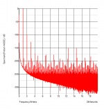
Just to make sure, I ran some sims Transient, Bode Plot, and
FFT using Simetrix and these models on a 1985 Elektor AXL
amplifier.
Attached is a FFT picture.
most simulations.
However, I do not know if these correctly simulate all and every
concievable parameter. I think they don't but that's another
story.
Just to make sure, I ran some sims Transient, Bode Plot, and
FFT using Simetrix and these models on a 1985 Elektor AXL
amplifier.
Attached is a FFT picture.
Attachments
I believe the transistor models I'm using are trustworthy then.
But isn't there anyone who's able to spot any obvious design flaws in my circuits? I managed to improve the performance somewhat (but still far from acceptable) by increasing the tail current feeding the differential pairs in the input stage, if that helps...
I also tried running a simulation in EWB with +/- 32 volt supplies and changing the resistor values in the output stage to those I'm using in my test setup (91 and 10 Ohms), and it still simulates perfectly, apart from the obvious fact that it'll clip at a lower signal level due to lower rail voltages.
Unless anyone's able to spot anything dramaticly wrong in the schematics I'm gonna put together the circuit on a PCB and using the real power supply with the correct rail voltages (I'm gonna put a current limiter on it to save the output devices if something goes wrong).
Hi Ventle
There might be a problem with the biasing of your vas stage. Current mirrors in a complementary differential stage cause the vas stage bias to be undefined. In a lot of instances the amp will still work but youll have dc offset problems. Slone used the mirrors in his early designs but most probably didnt build them and based them on spice. Everything is great with spice as it doesnt take into account the variations in actual components. In all his present designs which he has sold for comercial porpose he has dropped the current mirrors and uses resistors.
There are a lot of threads on this subject here, do a search on the name randy slone where these problems have been discussed.
Did you mesure the voltage across each of those output resistors? If you only measured .43v across the bias transistor
that sure points to a problem there either you need to replace it with the correct value, adjust it or have a bad transistor. I think
that outpur circuite wil need over 1 volt just to turn the drivers on.
So you are running in class B and a poorly biased class B.
that sure points to a problem there either you need to replace it with the correct value, adjust it or have a bad transistor. I think
that outpur circuite wil need over 1 volt just to turn the drivers on.
So you are running in class B and a poorly biased class B.
Sorry ment to say you probably need to replace that pot
with the correct value to get the bias circuite to work right.
with the correct value to get the bias circuite to work right.
thanks, that's quite useful information, meaning there IS a serious design flaw (I did search and read some long and quite informative threads about this design).
Seems like mr. Slone has found a way to overcome this limitation as well - the amplifier he only names 6-21 in his other book "The audiophile's project sourcebook" (known as the "OPTI-MOS" on the internet, see shcematics here) has been built by both Slone himself and several users on this forum. I actually breadboarded this circuit as well, but it turns out that this circuit won't work at all with 32-volt supply rails... PCB version with 66-volt rails coming up!
edit - this post was a reply to homemodders post 🙂
edit 2 - woody, I agree with your point, however, the scope traces does not indicate class B operation (no visible crossover distortion). I hooked up a 1.2 kOhm resistor in parallell with the pot, and the resistance value seemed to be correct, furthermore, I adjusted it to get the correct bias current through the output resistors, but results still the same - smooth curves with no speaker connected, massive distortion with speaker connected. I think homemodder has pointed out the real problem.
The optimos is very fine sounding amp ive got a built one, as a double complementry input stage where you can use current mirrors on its inputs is the design by stochinno. He ads a current source to the vas to define it. That design is also on some threads here and a better sounding amp but quite more complicated. Its one of the best sounding amps around these pages.
The slone amp can be made to sound a little sweeter and IMHO better to listen to soft rock, jazz or classical by some tweaking of the compensation but youll be happy with the sound that it already produces.
Have fun constructing
Alex
The slone amp can be made to sound a little sweeter and IMHO better to listen to soft rock, jazz or classical by some tweaking of the compensation but youll be happy with the sound that it already produces.
Have fun constructing
Alex
Interesting, i took a second glance at your vas stage, does slone show that cascode as in your schematic. The biasing of that cascode is a very clever trick to reduce high frequence distortion, Rotel uses it as well. I havent seen it done with a cfp before though. With lower rails it would be a problem with the optimos.
Hi
I wonder if the stange noise when the load is connected is due to the driver (VAS load) being starved of base current above the limit of the CCS(s) that is in series with the VAS load. If the CCS is uses to define the VAS bias Q point, it can only "sink" current below the bias point and not "source" it. Of course, as you know, without them the VAS bias will be undefined when using mirrors in the comp input diff.
I wonder if the stange noise when the load is connected is due to the driver (VAS load) being starved of base current above the limit of the CCS(s) that is in series with the VAS load. If the CCS is uses to define the VAS bias Q point, it can only "sink" current below the bias point and not "source" it. Of course, as you know, without them the VAS bias will be undefined when using mirrors in the comp input diff.
I see Slone mentioned by a poster.
Is this amp based on some of Slone's ideas?
Dual complementary VAS with current mirrors on the LTP does not work.
Is this amp based on some of Slone's ideas?
Dual complementary VAS with current mirrors on the LTP does not work.
homemodder said:Interesting, i took a second glance at your vas stage, does slone show that cascode as in your schematic. The biasing of that cascode is a very clever trick to reduce high frequence distortion, Rotel uses it as well. I havent seen it done with a cfp before though. With lower rails it would be a problem with the optimos.
Yes and no, he does use this VAS topology, but he doesn't bias the cascode transistor the way I've done it. I'm biasing it with a voltage divider setting the bias to exactly half the difference between the output rail and the supply rail - precisely as he has done in the optimos design (that's where I got the idea from).
I did notice the references to the stochinno amp in the other threads, I'll take a deeper look into it 🙂
AndrewT - yes, this design is based on Slone's work and yes, I've learned the lesson on complementary topologies with current mirrors by now 🙁
I like that cascode idea of yours, it might have some merits to it, and perform its intended purpose better than slones way. The best way for you to experiment with it would be to replace the current mirrors with resistors to solve that problem, then see how well that cascode scheme works and pinpoint the best bias setting for it. In spice where it sims as a working circuit does it perform better than slones??
I have some info on that cascode technique and how it operates as well as the patent taken out on it, but havent looked at it in some time, if you interested i will try to dig it up out of my hardrives. This goes for the stochino amp as well. ts been 4 5 years since i constructed these but i should still have all the research i did saved somewhere.
I have some info on that cascode technique and how it operates as well as the patent taken out on it, but havent looked at it in some time, if you interested i will try to dig it up out of my hardrives. This goes for the stochino amp as well. ts been 4 5 years since i constructed these but i should still have all the research i did saved somewhere.
- Status
- Not open for further replies.
- Home
- Amplifiers
- Solid State
- My Mosfet amp: why isn't it working?