Hey everyone. I've been DIY Audio member for about 10 months, more as a lurker, and I decided that today is great day to put in my two cents. I've worked on numerous audio projects but never a solid state amplifier. I’m hoping that my efforts on this amplifier will be a spring board to my own kit operation which I’ve been thinking about for sometime now.
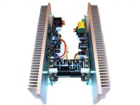
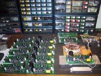
So to get started instead of trying to reinvent the wheel I decided after doing some research to go with a classic three-stage topology biased in Class AB. A differential stage with a current mirror for the input stage, voltage amplification stage, and EF output stage. By far the most challenging part was the board layout. But after several layout iterations, prototypes, and many hours of tweaking and listening, I'm very pleased with the results. The prototype boards have been in my system since November and sound incredible so I had Advanced Circuits make 25 professionally made boards with 2oz copper traces. I assembled and tested eleven boards, I kept a pair for myself, and the other four pairs are available to anybody who wants one at near cost. For more info email me at alsaudiokits@yahoo.com.
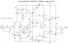
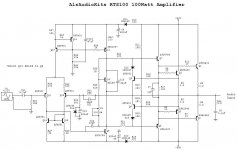
The amplifier which I’ll call the RTS100 delivers 105 watts into 8 ohms, 210 watts into 4 ohms. Has a frequency response of 2.5Hz to 205Khz, with a damping factor greater than 500 into an 8 ohm load after the output relay, and over 1500 before the relay at 1Khz. The relay has terminal lugs for easy bypass for those who hate relays. The amplifier is incredibly stable. I did put in provisions to add a zoble network but after some testing with an 8 ohm load in parallel with a variety of capacitors values at different power levels I found it’s not necessary. Signal to noise ratio measures at greater than 100db. There's also provisions for short circuit and thermal protection. Anyway, enough said. I’d like to here from you all. I’ve posted the schematic and will follow up with some pics.
Attachments
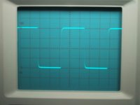
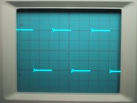
AAK: A very neat job, congratulations! The squarewave scopeshots look extremely good, but then you do have a 200kHz bandwidth. If I may suggest, limit the bandwidth deliberately to around 50-75kHz with an input RC to reduce the effects of stray pickup and RFI.
What made you decide on bipolar output devices instead of MOSFETs?
You mention short circuit protection, but unless I missed something, I don't see any actual overcurrent protection mechanism on the output stage. What will prevent 😱
😱  if one were to short the speaker terminals? If there's a possibility of damage to the amp with a short across the LS, Murphy's Law guarantees that such a short will happen. Sooner or later. . . Robustness is all.
Regards
John H
What made you decide on bipolar output devices instead of MOSFETs?
You mention short circuit protection, but unless I missed something, I don't see any actual overcurrent protection mechanism on the output stage. What will prevent
 😱
😱  if one were to short the speaker terminals? If there's a possibility of damage to the amp with a short across the LS, Murphy's Law guarantees that such a short will happen. Sooner or later. . . Robustness is all.
Regards
John H
Hi John, thanks for the reply and the suggestions. Actually the first RTS100 prototype used mosfets for the OS. I switched to BJTs primarily for economic reason. Lateral mosfets aren't cheap and unless you buy many there difficult to match. But If I where to build a more powerful amplifier 250 watt and up i would go with lateral mosfets.
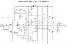
I've attached a revised schematic that includes short circuit protection that's implemented on the RTS100.
Best regards,
Al
I've attached a revised schematic that includes short circuit protection that's implemented on the RTS100.
Best regards,
Al
Attachments
Nice work
I have a question
210W into 4 ohms that is more than 10A. Unless the output transistors have a higher gain than about 25, it means a base current of 400 ma! Are Q7 and Q8 mounted on heatsink too (20W dissipation)? How the driver stage (Q7 , Q8) can work in class A with only about 10 ma DC?
I have a question
AAK said:...
The amplifier which I’ll call the RTS100 delivers 105 watts into 8 ohms, 210 watts into 4 ohms....
210W into 4 ohms that is more than 10A. Unless the output transistors have a higher gain than about 25, it means a base current of 400 ma! Are Q7 and Q8 mounted on heatsink too (20W dissipation)? How the driver stage (Q7 , Q8) can work in class A with only about 10 ma DC?
Hello AAK,
Good work - you've certainly swung into production! Square waves look good and ringing seems fairly well damped, but you need to do the C tests with at least 10Vrms AND larger C's AT 10KHz - someone else will so it's better you know if it's stable there. You may just need that zobel.
A few small criticisms -
1) Your THD and distortion character is not mentioned
2) Conventional miller C will load your 6mA Vas and will degrade -ve supply rejection. Two pole or feedback comp would be much better. Throws the onus for performance onto the PS.
3) Given min beta output devices your driver will need to deliver twice the standing current for rated power into 4 ohm to the output stage - so is not in class A.
4) Your short circuit protection appears to limit output current at zero volts to around 5A PER DEVICE but they are only 150W fragile 30MHz devices with a 150C max so derate heavily to around 100W or 2A at 50V each reliably.
5) The protection circuit has it's operating transistor biassed at 0.4V at zero crossing and almost on for the whole 'off' half cycle. This could affect the operation of the Vas /amp in normal operation.
Hope this is some help.
Hi AAk
I think that was a good idea , to use some degeneration , in a form of a resistor in the emitter of Q9 . Because now, Q14 is with less than 0,6 Volts between collector and emitter...
I think that was a good idea , to use some degeneration , in a form of a resistor in the emitter of Q9 . Because now, Q14 is with less than 0,6 Volts between collector and emitter...
Try 40V at 1KHz square wave into 4 ohms and you may see current limitation....Make sure you have the power supply to drive that amount of power though.
Absolutely Tube Dude!
How'd I miss that. Emitter degen for Q9 to raise base voltage AND limit current. somewhere around 50 -100 ohms would do. Around 68 ohms say should give fairly symettrical clipping allowing 50% Ic modulation. You could probably use this R as a clamp sensor to limit overload/protection current.
How'd I miss that. Emitter degen for Q9 to raise base voltage AND limit current. somewhere around 50 -100 ohms would do. Around 68 ohms say should give fairly symettrical clipping allowing 50% Ic modulation. You could probably use this R as a clamp sensor to limit overload/protection current.
amplifierguru said:Absolutely Tube Dude!
One more...how about a ~ 5k resistor between the collector of Q 17 and the common point of the emitters resistors of the LTP R 32 and R 33.
That way , we can isolate the summing point of the LTP , from the nonlinear output capacitance of Q17 collector and diminishing the transistor dissipation .
Yes it's a fair dissipation in Q17 - 250mW will drop Vbe for the second stage current source. Add another mA to that Vas Ic.
Al's running the high first stage current to supply that miller comp 47pF, hang the bias currents.
You can use 5K as you say Tube Dude to reduce dissipation. I'd cascode a BC55x off the 47uF decoupler for 10c, and really up that tail Z.
Greg
Al's running the high first stage current to supply that miller comp 47pF, hang the bias currents.
You can use 5K as you say Tube Dude to reduce dissipation. I'd cascode a BC55x off the 47uF decoupler for 10c, and really up that tail Z.
Greg
Hi fab,
I believe 210 watts into 4 ohms is about 7.25A if my calculations are right. The hfe for both OS devices are higher than 25. While matching transistors in a batch of about 50 for each device I measured hfe on average between 70 to 90 for the 2SC5200, and 100 to 120 for 2SA1943.
Best regards,
Al
I believe 210 watts into 4 ohms is about 7.25A if my calculations are right. The hfe for both OS devices are higher than 25. While matching transistors in a batch of about 50 for each device I measured hfe on average between 70 to 90 for the 2SC5200, and 100 to 120 for 2SA1943.
Best regards,
Al
Hi AAK,
Nice construction dude,
I am feeling little bit of jealousy from your nice production rig unit.😀 😀 😀
one thing is for sure , Your Current gain is very less.
You could use another pre-driver stage or you could use very high gain devices to ensure good current gain. in my opinion use an extra emmiter follower pre-driver stage to increase the current gain.
Also use emmiter degeneration resistor for VAS transistor.
Secondly, you could simply connect the compensation capacitor from collector of VAS transistor to base of differential transistor on the feedback side, as this would provide less phase shift and load the transistors collector lightly..
The current mirror formed at differential may cause parasitic oscillations [since the VCE of transistor forming CM is quite low]when signals with input frequency above 40khz are present, but they are not present in music, but may be perhaps when power bandwidth testing is going on..........
And also insert a 270 ohm resistor in series with the feedback compensation cap "22pF" in order to ensure some finite impedance at high frequencies or Mr. Miller could do some nasty thing when the amp would be driving some Piezo tweeter horns.
regards,
Kanwar
Drive current for output devices
Hi AAK,
I supposed that you mean 210 W RMS (that is the standard to use RMS for power amp, maybe not car amp though...) in 4 ohms, so
P = V^2/ (2*R) -- > V = (P*2*R)^0.5 = 41 V
Iac = Vac/R = 41 /4= 10.25 A
With hfe of let say 80 for output transistor (these are good output devices gain wise speaking), you need about 128 ma from the driver stage.
Do not get me wrong, in my opinion the schematic is correct (but at least with RE in the VAS) but maybe more appropriate for Mosfet output devices where the actual current from driver stage could be sufficient to drive the input capacitance of the mosfet (at least usual lateral types). I may be wrong but, by precautions, try an output voltage of 40 Vac peak (80V p-p) into 4 ohms or even 8 ohms to verify the voltage shape and behavior of the amp. Do NOT try with C of 2.2 uF in parallel at that 40 Vac though because you will blow the cap (or else) and believe me the cap smells badddd ...for a long time...(ask my girlfriend...). With a C of 2.2uF you probably do not need to exceed more than 10 V to get an appreciation of the behavior of the amp.
good luck
AAK said:Hi fab,
I believe 210 watts into 4 ohms is about 7.25A if my calculations are right. The hfe for both OS devices are higher than 25. While matching transistors in a batch of about 50 for each device I measured hfe on average between 70 to 90 for the 2SC5200, and 100 to 120 for 2SA1943.
Best regards,
Al
Hi AAK,
I supposed that you mean 210 W RMS (that is the standard to use RMS for power amp, maybe not car amp though...) in 4 ohms, so
P = V^2/ (2*R) -- > V = (P*2*R)^0.5 = 41 V
Iac = Vac/R = 41 /4= 10.25 A
With hfe of let say 80 for output transistor (these are good output devices gain wise speaking), you need about 128 ma from the driver stage.
Do not get me wrong, in my opinion the schematic is correct (but at least with RE in the VAS) but maybe more appropriate for Mosfet output devices where the actual current from driver stage could be sufficient to drive the input capacitance of the mosfet (at least usual lateral types). I may be wrong but, by precautions, try an output voltage of 40 Vac peak (80V p-p) into 4 ohms or even 8 ohms to verify the voltage shape and behavior of the amp. Do NOT try with C of 2.2 uF in parallel at that 40 Vac though because you will blow the cap (or else) and believe me the cap smells badddd ...for a long time...(ask my girlfriend...). With a C of 2.2uF you probably do not need to exceed more than 10 V to get an appreciation of the behavior of the amp.
good luck
Hi Greg,
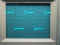
Thanks for all the great advice. Your C test is quite an extreme test, the chance of it being duplicated through the audio spectrum is quite small. But I guess it could happen, I'm glad that I put provisions for a zobel network on the board. The image below is the amplifiers output with a 2.3uF in parallel with an 8R at 10Khz at 10Vrms. It remained stable up to about 3uF. Beyond that it started blowing fuses. With the zobel network no problem.
Regards,
Al
Attachments
- Status
- Not open for further replies.
- Home
- Amplifiers
- Solid State
- My first solid state amp
