Hello people.
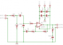
Below is my first non-inverted gainclone circuit. It is powered from a toroid-based power supply which will supply around 25-30v to it (still need to decide - any help will be appritiated). The power supply has 10000uf of total capacitence on each rail (shared by two copies of this circuit...)
I plan to power 6-8ohm speakers with it.
Volume controll will be established using an external, active, pre-amplifier yet to be built 🙂
Please - try be realistic. This is my first project - dont kill me 🙂
Thanks a lot 🙂 🙂
Attachments
Not sure what to say. It looks OK but I would use a smaller film capacitor for the DC blocker.
If you are using 10K caps in the PSU, I suggest that you have a look at Carlos' snubberized PSU. 😉
If you are using 10K caps in the PSU, I suggest that you have a look at Carlos' snubberized PSU. 😉
Heya.
I did put snubbers on the PSU 🙂
Ok, I will use a smaller capacitor. How about 4.7uF?
Except that. will it be ok?
Any other things worth adding/changing/removing?
Thanks.
I did put snubbers on the PSU 🙂
Ok, I will use a smaller capacitor. How about 4.7uF?
Except that. will it be ok?
Any other things worth adding/changing/removing?
Thanks.
How about 4.7uF?
That's fine and do make sure it is a good film type as this is the most important cap as regards sound quality. 😉
Anything else need changing? No, I don't think so but you can always read my thoughts on GC's at Decibel Dungeon. 🙂
eranrund said:Hello people.
Below is my first non-inverted gainclone circuit. It is powered from a toroid-based power supply which will supply around 25-30v to it (still need to decide - any help will be appritiated). The power supply has 10000uf of total capacitence on each rail (shared by two copies of this circuit...)
I plan to power 6-8ohm speakers with it.
Volume controll will be established using an external, active, pre-amplifier yet to be built 🙂
Please - try be realistic. This is my first project - dont kill me 🙂
Thanks a lot 🙂 🙂
Eranrund,
If you don't mind...a couple of suggestions:
1. I don't see a path for DC bias currents for the input. I would move C2 directly accross pin 7 and 8. Also move R2 to the other side of C1.
2. R3 and R1 are somewhat high in value, try 22K for R3, 1K for R1 and 100uF for C3.
3. The National application note for the 3886 mentions the potential need for a resistor accross the input terminals, at the input terminals to prevent oscillations when there is nothing connected to those input terminals. Leave yourself a spot on the PCB for a 10K or a 5K resistor and a small cap (to filter RF) right at the input terminals.
4. Try to get your feedback and input components closer to the 3875 chip on your circuit layout.
5. Provide separate ground returns to the star point of your chassis for signal ground (R2 and C3 return) than power ground (R4, C7, C8, C5, C6). Study the suggested layout for the 4870.
6. The power supply bypass capacitors need to be closer to the chip.
I have just finished putting together a 3886 board. When I first started it up I was using some linearly regulated supplies with test leads that were longer than I would have liked. In the process I discovered how sensitive the high gain, wide bandwidth chip is. I had oscillation issues with that test supply even though I had all of my bypass capacitors as close as physically possible to the chip, my feedback and input circuitry was in a tight loop around the chip pins, and I had separated my signal and power grounds all the way back to the star point.
When I switched to the real supply with shorter, heavier gauge wiring all of these issues went away, but it did give me a better appreciation for the warnings posted in the data sheet.
Scott
Heya.
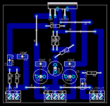
New versions:
- still need to figure out how to do star grounds - no idea how :-(
i think i'm gonna solder directly to the chip extra capacitors for +ve and -ve. i might solder the feedbacks on it as well.
Please give some more comments 🙂
New versions:
- still need to figure out how to do star grounds - no idea how :-(
i think i'm gonna solder directly to the chip extra capacitors for +ve and -ve. i might solder the feedbacks on it as well.
Please give some more comments 🙂
An externally hosted image should be here but it was not working when we last tested it.
An externally hosted image should be here but it was not working when we last tested it.
eranrund said:Heya.
New versions:
- still need to figure out how to do star grounds - no idea how :-(
i think i'm gonna solder directly to the chip extra capacitors for +ve and -ve. i might solder the feedbacks on it as well.
Please give some more comments 🙂
For an excellent example of star grounding look at the datasheet for the LM4870 (4780?). When doing your layout I suggest the following steps.
1. Place amplifier chip.
2. Place feedback parts next to the pins they are connected to.
3. Place input parts next to the pins they are connected to.
4. Place bypass parts next to the pins they are connected to.
5. Place everything else.
6. Route bypass capacitors with wide traces.
7. Route feedback nets keeping all traces as short as possible.
8. Route input nets keeping all traces as short as possible.
9. Route everything else.
Scott
I'm gonna retry that tommorow.
Too bad I'm a bit stuck since I'm doing single layer which makes some parts difficult to me.
I will look at the referenced datasheet tommorow as well.
Thanks again
Too bad I'm a bit stuck since I'm doing single layer which makes some parts difficult to me.
I will look at the referenced datasheet tommorow as well.
Thanks again
eranrund said:I'm gonna retry that tommorow.
Too bad I'm a bit stuck since I'm doing single layer which makes some parts difficult to me.
I will look at the referenced datasheet tommorow as well.
Thanks again
If you are stuck with a single layer run power and ground signals on the PCB layer and jumper signal traces as necessary. Use components wisely as your jumpers and you can get a lot done.
Scott
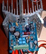
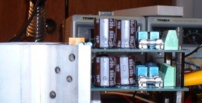
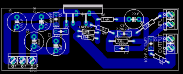
Some pictures...
For inspiration...here are some pictures of my 3886 board during testing.
R1, R2, R3, and R5 are the input and feedback resistors. The two orange boxes right next to the chip are .1uF bypass caps, followed by two 10uF, then farther away two 680uF bypass caps.
Minimum trace width in that area is 220mils for any length of distance, with some areas being 300+ mils. Wide is better for power traces.
Scott
Attachments
 !
!
eranrund said:A new version. Hope its better..
Much better! I see you studied the National data sheet!
I still see a couple more things that could cause you some issues when you build it...
1. C2 still needs to be placed accross pins 7 and 8.
2. R4 should be a 2W resistor it looks like it's 1/4W right now.
3. Copper on a PCB is free, the bypass caps copper return should be as wide as you can make it! 🙂
Scott
Hi 🙂
Ok, I will place C2 on the chip itself when I assemble this.
Are there any metal film 1% 2W resistors? Or can I just use a wirewound 5/10watt 10% resistor?
I planned on ordering the parts from www.futurlec.com
Perhaps you have a suggestion for another store to order the parts from? (To Israel)
I'll try making the bypass tracks wider. Is there any minimal distance between tracks that I should be aware of?
eranrund said:Hi 🙂
Ok, I will place C2 on the chip itself when I assemble this.
Are there any metal film 1% 2W resistors? Or can I just use a wirewound 5/10watt 10% resistor?
I planned on ordering the parts from www.futurlec.com
Perhaps you have a suggestion for another store to order the parts from? (To Israel)
I'll try making the bypass tracks wider. Is there any minimal distance between tracks that I should be aware of?
There is a minimal distance, and for a board without soldermask I don't remember what that is. I'd have to look it up. It's called creepage distance or just creepage. If you do a google search you might find it for bare conductors. Around 3-4 mm should do as long as your rails don't go over +/- 35V. That's a guess on the distance on my part...I don't have access to the U.L. or IEC rules and regs on that anymore. So I'm not even sure I could look it up.
I don't know about shipping to Israel, so I don't know who you could go with. A wirewound may or may not work there due to its inductance, depending on what the value of that inductance is.
I used the 2W version of these: http://www.mouser.com/catalog/specsheets/MO.pdf
Scott
- Status
- Not open for further replies.
- Home
- Amplifiers
- Chip Amps
- My first non-inverted gainclone circuit