Yes like that although you need to get a feel for the actual voltage needed on the FET gate and then decide on your final resistor values.
In your diagram you seem to have around 15 volts on the output. How are getting that ? It should be pretty much 0.0000 volts
Yes like that although you need to get a feel for the actual voltage needed on the FET gate and then decide on your final resistor values.
For that I need to know the voltage comming from the source?
So far I've borrowed alot of the values around the fet from the BCL clone schem.
Worth to mention is that I have not measured anything or powered on the circuit with vol.attentuator and/or input caps connected.
That might be worth doing before making alot of changes to the circuit?
Is it OK for the BC547B/BC547B (feeding the BD139/BD140) to get so hot after about 15min that I can touch them, but they're very hot?
I know they have a max dissipation of 300mW, I don't know how that "feels" though.
In simulation they dissipate nowhere near their limit.
In your diagram you seem to have around 15 volts on the output. How are getting that ? It should be pretty much 0.0000 volts
I think those figures are left from when I tried something that didn't work at all.
Changed back and took the screen shot without running the sim again.
I got a few uV in the simulations.
The DC voltage from the source equipment should always be zero. It would be a faulty unit that had any appreciable DC present.
It depends on the current through, and the voltage across the BCxxx transistors as to how hot they get. Confirm the current by measuring the voltage across the 68 ohm resistors and then calculate the current using ohms law. Multiply that current by the measured DC voltage across the transistor and you have the dissipation. 300mw would be pretty hot in a T092 package. But measure the values and then you know for sure.
I think you will find the transistors in the current source/sink get the hottest.
These type of circuits are very dependent on the actual characteristics of the transistors used and so you might need to tweak the resistor values around the output stage to get the currents you want.
I think those figures are left from when I tried something that didn't work at all.
Changed back and took the screen shot without running the sim again.
I got a few uV in the simulations.
That's more like it 🙂
Did not get anywhere near 0Vdc on the jfet board outputs.
Got to 1.3Vdc & 1.5Vdc
Then, this is the first thing to fix. If your jfets are truly matched, you should be able to trim the output to 0.
- Connect the input to ground with a 10K resistor.
- Start by disconnecting the diamond buffer from the jfet buffer (by removing R3 for example).
- Turn the trimmer all the way to its maximum value and then slowly turn it in the opposite direction while monitoring the output of the buffer.
You should be able to bring it to 0V.
The DC voltage from the source equipment should always be zero. It would be a faulty unit that had any appreciable DC present.
It depends on the current through, and the voltage across the BCxxx transistors as to how hot they get. Confirm the current by measuring the voltage across the 68 ohm resistors and then calculate the current using ohms law. Multiply that current by the measured DC voltage across the transistor and you have the dissipation. 300mw would be pretty hot in a T092 package. But measure the values and then you know for sure.
I think you will find the transistors in the current source/sink get the hottest.
These type of circuits are very dependent on the actual characteristics of the transistors used and so you might need to tweak the resistor values around the output stage to get the currents you want.
I'll look at replacing the 0805 68R's with 100R trimpots tomorrow.
Also have two other headamps to power on and measure DC offset etc on.
Thanks, I appreciate the help 🙂
I've got a transistor tester, but I don't actually know what to look for when matching BJT's.
The tester shows B and Vf.
Then, this is the first thing to fix. If your jfets are truly matched, you should be able to trim the output to 0.
- Connect the input to ground with a 10K resistor.
- Start by disconnecting the diamond buffer from the jfet buffer (by removing R3 for example).
- Turn the trimmer all the way to its maximum value and then slowly turn it in the opposite direction while monitoring the output of the buffer.
You should be able to bring it to 0V.
They are matched, all 3.7mA.
I'll look in to this as well tomorrow.
Thanks, your help is appreciated 🙂
Schematic and FFT (I'd say that it's decent).
With the 6.8uF, Do I need to change R13?
For testing/trimming jfet board, should I put 10K between the each 10K input resistor (will connect attentuator to them, input) and gnd?
About the hot TO-92's, I'm fairly shure it was Q1-Q2 that was hot, much more so than the CCS's.
The transistor tester I have(ATmega 328 based) gives two values,
B (three digit number)
and Vf (xxxmV).
If I where to swap the BC547B/BC557B for "matched", I have about 50 of each that I've tested with the thing and marked with the results.
I don't know what values to match though and if I find a number of transistors close to eachother, which range of that value that is prefered?
I hope I make myself somewhat understood, I just got out of bed and the coffee has not done it's magic yet.
With the 6.8uF, Do I need to change R13?
For testing/trimming jfet board, should I put 10K between the each 10K input resistor (will connect attentuator to them, input) and gnd?
An externally hosted image should be here but it was not working when we last tested it.
An externally hosted image should be here but it was not working when we last tested it.
About the hot TO-92's, I'm fairly shure it was Q1-Q2 that was hot, much more so than the CCS's.
The transistor tester I have(ATmega 328 based) gives two values,
B (three digit number)
and Vf (xxxmV).
If I where to swap the BC547B/BC557B for "matched", I have about 50 of each that I've tested with the thing and marked with the results.
I don't know what values to match though and if I find a number of transistors close to eachother, which range of that value that is prefered?
I hope I make myself somewhat understood, I just got out of bed and the coffee has not done it's magic yet.
Last edited:
Matching the bjt's isn't so important here, its more applicable to LTP and balanced input stages. Going for high gain devices is usually worthwhile though.
Matching devices can be done either at a basic level such as calculating gain for a given base current and observing the resulting collector current, or more ideally by plotting the characteristics with a curve tracer. This shows the general idea. Here you are plotting the results over a range of voltage across the device.
The Transistor Curve Tracer
Any respectable design should work correctly with devices from one extreme to the other... if its critical on components used then generally that's not good.
You need to decide what input impedance you want the circuit to present to the outside world in order to settle on the input value components. Generally, line inputs are made high impedance to avoid loading the source (say 100 to 500k). Noise isn't an issue because the high input impedance gets shunted by the low output impedance of the source component.
Matching the bjt's isn't so important here, its more applicable to LTP and balanced input stages. Going for high gain devices is usually worthwhile though.
Matching devices can be done either at a basic level such as calculating gain for a given base current and observing the resulting collector current, or more ideally by plotting the characteristics with a curve tracer. This shows the general idea. Here you are plotting the results over a range of voltage across the device.
The Transistor Curve Tracer
Any respectable design should work correctly with devices from one extreme to the other... if its critical on components used then generally that's not good.
You need to decide what input impedance you want the circuit to present to the outside world in order to settle on the input value components. Generally, line inputs are made high impedance to avoid loading the source (say 100 to 500k). Noise isn't an issue because the high input impedance gets shunted by the low output impedance of the source component.
I'm just about on my way out (getting my neck x-rayed) but I'll read through your post more carefully later.
The attentuator(50K) will be in front of the headamp, and there's the 10K input resistor.
I don't know if that presents an easy enough load for the source (DAC) that'll feed the headamp?
The 50k attenuator is variable I assume ?
Well yes, I get your point.
It's a so called Dact type stepped attentuator.
Maybe setting the input resistors to 50K-100K will make the headamp a reasonable load?
OK 🙂
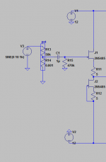
So, there could be a little problem here. R13 and R14 (via R2) appear as a 'load' on the wiper of the pot. That changes the law of the pot significantly. For example, as you have it now at the midpoint (25k + 25k) then for 1 volt rms applied to the input, you will only get around 32 millivolts at the gate of the FET.
So, there could be a little problem here. R13 and R14 (via R2) appear as a 'load' on the wiper of the pot. That changes the law of the pot significantly. For example, as you have it now at the midpoint (25k + 25k) then for 1 volt rms applied to the input, you will only get around 32 millivolts at the gate of the FET.
Try making R13 1meg and for now removing R14/C6. Now move the input cap so that it is in series with R2. This will prevent 'noise' from the wiper passing a small DC current as it is turned. As you have it now, the DC voltage from the servo is applied to the attenuator and not only that, as the attenuator is altered, the servo voltage will alter to as it 'fights' to keep the gate voltage of the FET constant.
Ok, so do the sim with different settings?OK 🙂
So, there could be a little problem here. R13 and R14 (via R2) appear as a 'load' on the wiper of the pot. That changes the law of the pot significantly. For example, as you have it now at the midpoint (25k + 25k) then for 1 volt rms applied to the input, you will only get around 32 millivolts at the gate of the FET.
I'll do this when I get home.Try making R13 1meg and for now removing R14/C6. Now move the input cap so that it is in series with R2. This will prevent 'noise' from the wiper passing a small DC current as it is turned. As you have it now, the DC voltage from the servo is applied to the attenuator and not only that, as the attenuator is altered, the servo voltage will alter to as it 'fights' to keep the gate voltage of the FET constant.
In the car(not driving) on my way to get my neck nuked.
I'll try it in sims, then post that and move on to real world changes.
Again, thanks for helping 🙂
Let's fix one thing at a time, please. Sims are not needed, it's a very simple circuit.
Just wire your buffer as shown in the attached schematic, nothing more connected and report.
r15 can be 330k to 1meg and c1 value isn't critical for now. Don't mind the 2n5485, that's all I had as model installed on this computer.
Just wire your buffer as shown in the attached schematic, nothing more connected and report.
r15 can be 330k to 1meg and c1 value isn't critical for now. Don't mind the 2n5485, that's all I had as model installed on this computer.
Attachments
Maybe it's time to ask Santa for a new Fiancé.................My fiance is not happy about me spending all day with the solder station, ................
the input in post38 is correct.
R15 sets the input impedance.
C1 is the DC blocker.
Compare to post30.
R14 sets the input impedance. do you really want 1k8 as your input impedance?
C2 is in the wrong position.
What is R2 =10k supposed to do?
This input is completely wrong.
Move C2 to next to R2
Change R2 to 2k or 100r or anywhere in that range.
C6 is the RF filter. For simulation of the circuit set it to 1fF
For filtering simulation set it to around 200kHz, i.e. RC = ~0.5us (500ns), 10k+6k5 & 100pF = 1650ns
For two perfectly matched J1&J2 the Rtrim must be set to 5r1 to exactly match R1 (5r1)
In the real circuit you can adjust until the output offset measured at J2 drain is 0.0mVdc. BUT this ONLY works when the DC block is present at the input and the DC servo is disconnected.
Last edited:
- Status
- Not open for further replies.
- Home
- Amplifiers
- Headphone Systems
- "My" first design headamp, DC-servo question