I could run a sim to see how much improvement the buffer makes... TL431s are so cheap here😛
that's a good idea. a comparison between the basic tl431, a buffered tl431, and a constant-current sourced and buffered tl431 would be very revealing. i'll work on the same thing here and see if i get anywhere.
~ brad.
tentative results
ok, i hacked together some schematics and a few bash and gnuplot scripts to compare line regulation of each topology. i've attached my tentative results as a pdf. i welcome feedback and opinions and questions. 🙂
the circuits:
vanilla tl431: a la figure 10 in the tl431 datasheet.
buffered tl431: a la figure 12 in the tl431 datasheet. bd244c as shunt bjt.
bjt super shunt: a la salas shunt. bd244c as shunt instead of irpf9240.
all circuits are followed by a 1000uF bypass cap and are designed around 3.3V output at 160mA load current.
~ brad.
Attachments
Last edited:
OK, guess you're using the Fairchild datasheet for your figures. I looked in TI first...
Your differences between the vanilla TL431 and buffered variant look similar to the results of my sim - i get 0.2ohm for the dynamic impedance of the vanilla and can get down to 10mohm with the buffered one. Your rejection plot I guess is limited by the series resistor you're using. So it would be fairer to compare the TL431 variants when fed with a current source. Anyway, excellent work!
Oh, a question - if all circuits are followed with a 1000uF, why doesn't the salas shunt benefit from the improved HF rejection given by the cap? (In reality, the 1000uF will have some ESR which will stop the indefinite HF roll-off).
Last edited:
if all circuits are followed with a 1000uF, why doesn't the salas shunt benefit from the improved HF rejection given by the cap?
an excellent question to which i have no answer. these results are what the sim has given me... 😕
~ brad.
well, for now i think i'll begin reworking the schematics to use ccs-fed bjt shunts as simulated...
while we're on the subject of power supplies, i'm starting to believe that there's no inherent advantage to completely separate unregulated power supplies for each section. i'm tempted to boil the power supply section down to, say, two trafos (one for 3.3v and 5v, one for 30v), two rectifier stages (again low-voltage and high(er) voltage), and then break each rail out using a separate regulator. it seems that many other dac designs on the forum follow this pattern. opinions here?
third, using a micro to control power relays is starting to seem like a hassle, so i may switch to DIP switches and a basic power switch...
~ brad.
LTSpice
Here's my schematic file for the buffered TL431 shunt, FWIW. I'm using LTSpice.
On power supplies, yes, agreement, subject to what you intend to do with the grounding. The only advantage of separate supplies (from separate transformer windings) is control of ground currents.
Here's my schematic file for the buffered TL431 shunt, FWIW. I'm using LTSpice.
On power supplies, yes, agreement, subject to what you intend to do with the grounding. The only advantage of separate supplies (from separate transformer windings) is control of ground currents.
Attachments
Last edited:
thanks, but i use linux exclusively so i cant open your circuit... 🙁
as for grounding, you are referring to the avoidance of ground loops by proper ground returns, etc, right?
~ brad.
as for grounding, you are referring to the avoidance of ground loops by proper ground returns, etc, right?
~ brad.
Oh, according to the guys at LT (the writers of LTSpice) it'll work under Wine. Or were you meaning you can't read a zip file with linux? If not, I can email it to you. The forum only allows a limited subset of extensions to be uploaded.
Yeah, ground loops at all frequencies from DC - light.
Yeah, ground loops at all frequencies from DC - light.
Last edited:
Oh, according to the guys at LT (the writers of LTSpice) it'll work under Wine. Or were you meaning you can't read a zip file with linux? If not, I can email it to you. The forum only allows a limited subset of extensions to be uploaded.
no, i can open zip files ok, i just haven't taken the time to fully figure out wine... 😛
Yeah, ground loops at all frequencies from DC - light.
haha, if i wasn't already nervous enough about designing in the HF band. 🙁
~ brad.
Shunt in progress
Here's the schematic for my progress so far with the 'low complexity shunt'. It achieves <10mohm output impedance from DC through 1MHz, at the expense of 3 fairly large value low ESR electrolytics across it. Test current is 10mA. Not sure how far to develop it above 1MHz. Any ideas?
Here's the schematic for my progress so far with the 'low complexity shunt'. It achieves <10mohm output impedance from DC through 1MHz, at the expense of 3 fairly large value low ESR electrolytics across it. Test current is 10mA. Not sure how far to develop it above 1MHz. Any ideas?
Attachments
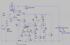
ok, from the looks of it, you are buffering the output of a discrete 'TL431' (or is that actually the guts of the TL431?) with a logic-level-gate mosfet... i see no ccs, though i may be blind... 😛 it looks good to me. 🙂
unfortunately, the fairchild spice model for the fdn304p is anything but cooperating with my version of spice (3f5), so i can't seem to simulate it using a css and zener reference. (why spice3 doesn't accept poly() syntax is beyond me...)
~ brad.
unfortunately, the fairchild spice model for the fdn304p is anything but cooperating with my version of spice (3f5), so i can't seem to simulate it using a css and zener reference. (why spice3 doesn't accept poly() syntax is beyond me...)
~ brad.
... unfortunately, the fairchild spice model for the fdn304p is anything but cooperating with my version of spice ...
it seems i spoke too soon. 😛 after rewriting the model's nonlinear dependent sources in a form which spice3f5 understands, i was able to simulate line regulation of the salas topology using the p-channel mosfet you used in your simulation.
results are posted with new data...
~ brad.
p.s. great work! thanks for all the help and information on this.
Attachments
Last edited:
revised input section
i figure i should go ahead and post each revised section as i work through the design...
attached is the revised input section. i removed the error signal output from the dir9001, as i've decided to take the micro out of the design. the dir operates in pll mode with a system clock of 512*fs for the lowest possible jitter. it's set to output 24-bit msb-first right-justified data.
the dir is now powered off the single +3.3v supply, with its vcc and vdd decoupled by a 1uH inductor. its dgnd and agnd are directly connected to the +3.3v ground.
~ brad.
Attachments
revised reclock section
here is the revised asrc section. i switched to the src4192 to remove the micro from the mix. switches toggle bypass and select between 48khz/96khz output sample rates. the asrc input format is 24-bit msb-first right-justified, and so is the output format. the normal group delay setting is used.
again feel free to note design errors or possible corrections or modifications as i post these schematics...
~ brad.
Attachments
revised dacs section
the section for the dacs has mostly been cleaned up. for instance, the positive power pins are above the negative pins now, so the decoupling caps are right-side-up. the dacs will be operating at 8x oversampling, so they will run at 768khz.
~ brad.
the section for the dacs has mostly been cleaned up. for instance, the positive power pins are above the negative pins now, so the decoupling caps are right-side-up. the dacs will be operating at 8x oversampling, so they will run at 768khz.
~ brad.
Attachments
revised i/v converters
the i/v converters still use the sample topology of the mosfet pass d1 w/ fet-ccs-loaded output stage, but i removed the 10R resistors on the power rails as they negate the low output impedance of the salas shunts.
more to come as i rework the power supplies and regulators. (i'm planning for now on using low-voltage salas shunts, either with a bd244c or fdn304p as an output device.
~ brad.
Attachments
revised i/v power supply sections
ok, here are the power supplies for the i/v converter. using a dual 15Vac toroid with secondaries in series, i can get 42Vdc unregulated out of the rectifier, under load.
the difference here is that now only one RCL filter (R701, C701/2/3, L701) is present, so all three (two for iv, one for lv) transformers connect to MAINS_LIVE and MAINS_NEU from this filter. i also increased the inductance of the common-mode choke in the filter.
~ brad.
Attachments
- Status
- Not open for further replies.
- Home
- Source & Line
- Digital Line Level
- My Complete Solution DAC, RFC