Hi E'body, thx for your answers.....I've measure the current diff. between two amps, the good one has voltage difference about 60 mv on R23, R24 & R27, R28 (2 ma biasing) and DC offset about 5 mv , but the bad one has 60 mv on 60 mv on R23, R24 and 256 mv on R27, R28 ( it has 4 ma difference) and the offset is always negative voltage ( about -800 to -4 V), is there probably any comp. breakdownn or oscillation??
Thx for your help.....
Lukio
thx for your help
Thx for your help.....
Lukio
thx for your help
Attachments
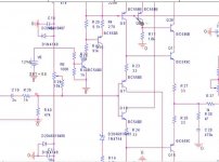
Maybe set R29, the DC offset control in the middle and get back to us with the voltage readings at the bases and emitters of the input transistors (Q7 and Q?) as well as the voltage at the intersection of R27 and R28. Also check the voltages across R23,24,27, and 28--or even better, give the currents through each of those resistors using the formula I=V/R.
Voltage reading
Hii.. Subwo1
Thx alot for your reply.....
After measure there are different on voltage between the good one and the bad one. The good one has voltage different about 70 mv on R23, R24 (R base Q11,Q12) & R27, R28(R emittter Q11,Q12) and 1.2 V on R1, R15 (R Colector for Q1,Q12) (about 2.5 ma run) that close enough from calculation but the bad one have voltage diff. about 70 mv on R27,R28 (R base Q11,Q12) & 1.9V on R1,R15 () (R Colector for Q1,Q12, 4.5 ma run) but about 240 mv on R23, R24 (R emittter Q11,Q12, about 7 ma run) there is big current different between Colector Q11, Q12 (4.5ma) and Emitter on Q11, Q12 (7 ma) (Q11&Q12 are input transistor). If these problem caused by oscillation, does it necessary to place miller cap between Collector Q33 and base Q5 and vise versa for Q32 and Q6 (Driver stage)??
Best regards,
Lukio😉
- Status
- Not open for further replies.