digi01 how u build so professional PCB? thats amazing 🙂
wich method u use? u have some machine to do that?
can u tellme some link abt the hardware or how u build that stuff?
thanks
wich method u use? u have some machine to do that?
can u tellme some link abt the hardware or how u build that stuff?
thanks
He uses regular pcb CAD software which can create Gerber files. Those files are then given to a pcb factory.
Hi digi,
one newbie question about your design, which BTW I think looks really very nice: what goes into the null pads and what does it do?
thanks
one newbie question about your design, which BTW I think looks really very nice: what goes into the null pads and what does it do?
thanks
thank you.
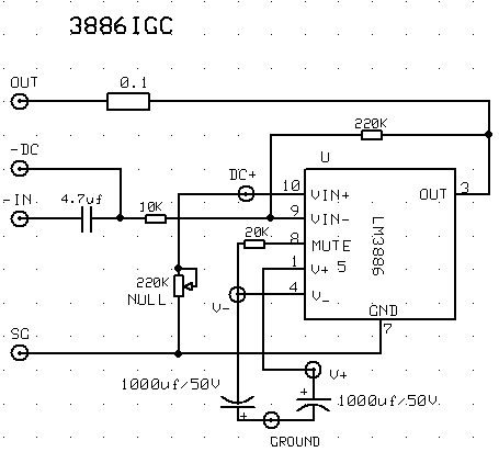
I like substantial pads on both sides of the board for any connections. the null pads for installation unused pins of LM3886.those NC pins do not need pads but they need holes.
I like substantial pads on both sides of the board for any connections. the null pads for installation unused pins of LM3886.those NC pins do not need pads but they need holes.
Hi digi01-
I think he was referring to the three holes with the silkscreen rectangle around them labeled "NULL".
The place is next to the mounting hole.
My guess was a 10 turn pot since it is labeled with an Ohm value and has 3 holes.
Thanks,
Troy
I think he was referring to the three holes with the silkscreen rectangle around them labeled "NULL".
The place is next to the mounting hole.
My guess was a 10 turn pot since it is labeled with an Ohm value and has 3 holes.
Thanks,
Troy
thank you rabstg,maybe you are right🙂
"null" in chinese sounds like "turn".
you can put a 10 turn pot(220k) on the "NULL" pad.it is set up to adjust output dc drift.can short it in normal used.
goering said:Hi digi,
one newbie question about your design, which BTW I think looks really very nice: what goes into the null pads and what does it do?
thanks
"null" in chinese sounds like "turn".
you can put a 10 turn pot(220k) on the "NULL" pad.it is set up to adjust output dc drift.can short it in normal used.
Wanna post a high resolution layout? As in a seperate image for top, bottom and silk-screen layers. Pretty please? 
Edit: On a side note, how wide is the offset adjust range?
Edit: On a side note, how wide is the offset adjust range?
here is 3886 gianclone partlist:
2 PCBs for stereo amp:
3886igc PCB *2
1000uf/50v *4
LM3886 *2
220k 1/2w *2 (gain setting)
10k 1/2w *2 (gain setting)
20k 1/4w *2 (mute)
0.1/5w *2 (option,can be shotr.for output)
220k trim *2 (option,can be shotr.for dc offset)
heat sink,screw,hook wires.
enjoys
2 PCBs for stereo amp:
3886igc PCB *2
1000uf/50v *4
LM3886 *2
220k 1/2w *2 (gain setting)
10k 1/2w *2 (gain setting)
20k 1/4w *2 (mute)
0.1/5w *2 (option,can be shotr.for output)
220k trim *2 (option,can be shotr.for dc offset)
heat sink,screw,hook wires.
enjoys
Hey digi01-
Quick question.
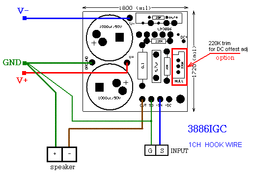
The dimensions of the board, they are 1800 x 1720 Mils. That can't be mili METERS can it?
Thanks again in advance,
Troy
Quick question.
The dimensions of the board, they are 1800 x 1720 Mils. That can't be mili METERS can it?
Thanks again in advance,
Troy
Mils is standard in the pcb cad business and is 1/1000 of an inch.
1.8 x 1.72 inch 😀
... and the reason for using mils is that the programs in the early days had 32000 x 32000 or 32768 x 32768 as max values of the coordinates. This gave us 32 x 32" as max board size. Worth noting is the program "Boardmaker(?)" or something had 4 x 4 billions in max values. The resulation was 0.1 um and was used for silicone chips. It ran on Mac in the 80's and could be connected to a mainframe. Those where the days.
Hey peranders-
Rgr that and thanks for the clarification.
As the saying goes, "more about Penguins than I wanted to know".
But thanks for the history.
Troy
Rgr that and thanks for the clarification.
As the saying goes, "more about Penguins than I wanted to know".
But thanks for the history.
Troy
BTW,100mil is standard in the common electronic parts.
for example:
the caps leg always in 200/300/400(mil) and 100mil=2.54mm.
another:
like the holes board,the distance between every hole is always 100mil.
-digi
for example:
the caps leg always in 200/300/400(mil) and 100mil=2.54mm.
another:
like the holes board,the distance between every hole is always 100mil.
-digi
the board is available now.
link:http://www.diyaudio.com/forums/showthread.php?s=&threadid=41746
enjoys
digi
link:http://www.diyaudio.com/forums/showthread.php?s=&threadid=41746
enjoys
digi
- Status
- Not open for further replies.
- Home
- Amplifiers
- Chip Amps
- my 3886IGC pcb