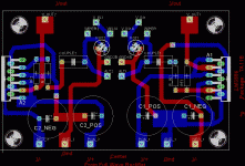
Below are pictures of my PCB layout for a stereo amp based on the 3886 chip (inverting configuration like Peter Daniel's and others). I'm just posting this to get comments from everyone prior to actually making the board. Do you think it will work? Obviously the values are not in there, but assume I use the standard values posted by I think Thor and Peter Daniel. This is done on Eagle.
The point of this PCB is to get something that works so I can play around with it a little and get familiar with chip amps. I don't have a rectifier board, this connects after the rectifiers.
1. In particular, are the pins of the 3886 chip connected correctly? I think that they are, and hope that I got the orientation correct. If you can verify this that would be great.
2. I have made this for a pcb mounted attenuator, but left connection points for external attenuators, so that is why you see extra points for "wiper" and such.
3. Also made a provision for a larger coupling capacitor, so you see an extra hole for that too.
Comments appreciated, and yes, this is my first ever PCB design.
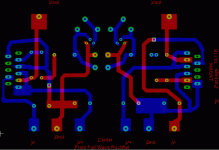
I think you should identify all high current traces and make them wider. The LM3886 can handle at least 11.5 A.
- Status
- Not open for further replies.