Cool, thanks - it looks very compact at first glance. Which version of Eagle-PCB do I need, to work on it?
I'm not realy into simulation... so, I have question...
I see many capacitors in series with low value resistors like 0R02... is this just for simulation or is it an intended component...
PS, I am makeing a nice layout now useing SOT223 packages... (they are maybe even slightly larger than the cans)...
I see many capacitors in series with low value resistors like 0R02... is this just for simulation or is it an intended component...
PS, I am makeing a nice layout now useing SOT223 packages... (they are maybe even slightly larger than the cans)...
R21, R22 and R22 are parasitics - approximate ESR of the capacitors, meant only for simulation. Likewise, R26 and R27 are the approximate lead resistance from the PSU board to the amplifier board, again for the simulation (I should probably have used different notation for the parasitics, I noticed that you've placed and routed the parasitics also on your layout). Everything else is a real component.
I'm changing a few components, removing the parasitics and moving things around on your layout. The main changes are capacitor values and diameters, and replacement of the integrated current mirror with discretes. I will also try to route as much as possible on one layer, leaving just a few unavoidable jumpers.
The main problem I'm facing is that the free version of Eagle 4.16 seems to have a minimum snap-to grid value that is larger than what you used, making some angled routes impossible to route at nice (45, 90, 135 degree) angles. I think I can work around it, let me see how it goes...
Anyway, this is the first time I'm using Eagle, and I must say that its use-model is very impressive, in particular the simultaneous Schematic/Board design flow - which allows deletion and addition of components, etc. on a partially placed and routed board, without losing the netlist/rat's nest. Completely different from the old OrCad for DOS design flow.
Big sigh of relief....
Can you show resistor dissipation as well with your sim program...?
I am just working on rough guesses so far...
Excuse me going all SMD on the project, it is some practice... First time I made working new library components...
As you can see the transistors are realy big for SMD stuff...
Which brings me to another question... The 2n2222s etc used I guess were pretty hot at the time of design, but surely there has to be better devices by now?
P.S. it is notfinished yet.. just a snapshot of were I am at now.
Attachments
R23 is 1W, R25 is 5W. Everything else can be 1/4 W.
The electrolytics (numbering as per my schematic) are:
C4: 100uF, 25v; 8 mm should be fine.
C5: 330uF, 50/63v; 10 mm should be ok, 12 mm by way of abundant precaution.
C11, C14: 1800uF, 25/35v; 12 mm should be ok. (I forgot to add a film bypass cap in parallel to these. You can put a 100nF film in parallel with both these).
C7: 330uF, 6.3v or higher; 10 mm.
C8: 9900uf, 6.3v consisting of 3 x 3300uF, 6.3v in parallel (again missed showing the caps in parallel on LTSpice schematic). 4 x 12mm should cover any need for a 4th cap in parallel.
The other caps seem to be ok - you may want to leave enough width for the small caps to allow the use of polystyrene, silver mica or box-type polyester as needed. In particular, the input coupling cap (C1) outline can be made much larger to allow the use of bulky Axial-lead Teflons/Paper-Oil/Polyprops, etc., as necessary.
Edit: The 2n2222/2n2907 are because of the included small-signal LTSpice models - you can safely substitute any small signal device with Vceo > 50v, including the following:
2n2222: bc548/549/550, bf422, 2sc1815, 2sc1845, 2sc2240, mpsa42, ...
2n2907: bc558/559/560, bf423, 2sa1015, 2sa992, 2sa970, mpsa92, ...
For Q3, 2sc2705 is probably best, but any of the NPNs above should work. Also add an outline for a Miller cap of ~27 pF between B-C of Q3.
I'm also running into the 100mm x 80 mm limitation of the free version of Eagle, so I'm going to make the PCB wider and shorter (i.e. more square) and move the components accordingly. This will also help to spread the FETs apart on the heatsink, and manage the power dissipation (~2 x 30W, quiescent) better.
If my calculation is right the resistor connecting the input pair to the positive rail will run at 0.24W, I reccon that one should be uped in wattage, or two packages paralleled.
Thanks, reducing the grid value to 0.3175 mm from 1.27 mm seems to have helped greatly.
I overlooked R7 - 1/2 W should be fine.
I overlooked R7 - 1/2 W should be fine.
I am now bussy dropping down from SMD back to through-hole...
Lots easier than going the other way around...., I am keeping the smd transistors though... I think they look neat...
Lots easier than going the other way around...., I am keeping the smd transistors though... I think they look neat...
LXG,
Brilliant work!
Nordic,
Exquisite layout, you are going from strength to strength!!
I would urge you to build this amp. I really like the circuit and I'm convinced it would better Le Monstre.
Cheers,
Hugh
Brilliant work!
Nordic,
Exquisite layout, you are going from strength to strength!!
I would urge you to build this amp. I really like the circuit and I'm convinced it would better Le Monstre.
Cheers,
Hugh
AKSA, thanks for your kind words. Nordic, thanks for your good work on the SMT PCB and giving me a nice head-start on the through-hole version. I wrestled with it until 3 AM - the modified placement is almost done, and the remaining rat's nest looks very manageable now. I'm confident that all tracks will route in one layer, and will be reasonably short and smooth.
Hi Hugh, you will give me a big head 😀
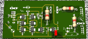
Attached find the through hole version of my board.
On comparing the datasheets for the leaded and SMT components, it was clear the through hole ones had quite an advantage in both dissipation, and gain...
Attached find the through hole version of my board.
On comparing the datasheets for the leaded and SMT components, it was clear the through hole ones had quite an advantage in both dissipation, and gain...
Attachments
Nordic,
You're really good on designing circuit boards. How long you've been doing this?
You did an awesome job!

You're really good on designing circuit boards. How long you've been doing this?
You did an awesome job!
Think I have been at it since early 2006...but most of the learning was over the last year.
Yesterday I tried the new eagle 5 trial (cough cough, any licenceing help would be appreciated)....
I would say it will have a much faster learning curve than the older versions... also check out the what's new information as it provides a config line that enables you to do group selection in stead of menu, on right clicking, like the old versions.
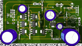
I attach an optimised version of the board in Eagle 5, you will need Eagle 4.6 as a minimum to open these files..... Luckily the board is small (92x67mm) enough to fit in the trial size limits(100x80).
Remember to hit the Ratsnest button to fill polygons or simply type the word ratsnest and hit enter in PCB view.
Yesterday I tried the new eagle 5 trial (cough cough, any licenceing help would be appreciated)....
I would say it will have a much faster learning curve than the older versions... also check out the what's new information as it provides a config line that enables you to do group selection in stead of menu, on right clicking, like the old versions.
I attach an optimised version of the board in Eagle 5, you will need Eagle 4.6 as a minimum to open these files..... Luckily the board is small (92x67mm) enough to fit in the trial size limits(100x80).
Remember to hit the Ratsnest button to fill polygons or simply type the word ratsnest and hit enter in PCB view.
Attachments
Nordic, that looks great - far more compact than the first through-hole version, which I've now modified, added a few small caps and finished routing. I couldn't get rid of one jumper, so it remains (as a single track on the component side, which won't actually be printed, but instead be replaced by a jumper during assembly).
BTW:
1) Does Eagle 4.16 have an option to view the rendered 3D image of the mechanical model, as you've shown? I couldn't locate it.
2) Which is the best option for laser-printed solder-side artwork, with only
tracks, pads, vias and outine (or dimension markers)? Is a postscript or
EPS file good enough? (The reason that I'm asking is that there are
small-run prototype PCB makers here who can work with just a
laser-printed paper image instead of a gerber file - and it costs far
less to make single-sided PCBs with the paper-image).
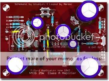
Here's the schematic and fully routed PCB of my modified through hole version, which I'm calling MullardV2:
BTW:
1) Does Eagle 4.16 have an option to view the rendered 3D image of the mechanical model, as you've shown? I couldn't locate it.
2) Which is the best option for laser-printed solder-side artwork, with only
tracks, pads, vias and outine (or dimension markers)? Is a postscript or
EPS file good enough? (The reason that I'm asking is that there are
small-run prototype PCB makers here who can work with just a
laser-printed paper image instead of a gerber file - and it costs far
less to make single-sided PCBs with the paper-image).
Here's the schematic and fully routed PCB of my modified through hole version, which I'm calling MullardV2:
Attachments
- Status
- Not open for further replies.
- Home
- Amplifiers
- Solid State
- Mullard SS power amplifier