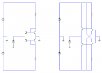
The two most obvious bias schemes for BJT are attached. First is the simple pair of diodes (or diode connected BJTs in this case). Second is the 'diamond buffer', which is the best way I can think of.lumanauw said:...How to implement your idea, if the front end is not JFET (Bipolars for instance) without adding complexity?..
I think I can see how that works. I'd be worried about thermal stability though.lumanauw said:Mr. Evil,
Since you like to acrobat with schematics😀 what do you think of my non-turnoff bias scheme? D2 is used by both T1 and T2
Attachments
Hi, Mr.Evil,
In the diamond buffer drawing, the base of the left transistor(s) are driving emitors of right transistor. Is it can really work ? Looks like a reversed process to me (the signal should come from right transistors, but if we do this, the signal will come to bases)
In the diamond buffer drawing, the base of the left transistor(s) are driving emitors of right transistor. Is it can really work ? Looks like a reversed process to me (the signal should come from right transistors, but if we do this, the signal will come to bases)
Both schematics are kind of backwards, the voltage source is where the load normally would be and the ground on the right is the input.
Edit: Now that I've gone back and read the first two pages.
What advantage is there to applying the signal to an emitter rather than a base? The signal still appears across B-E.
Edit: Now that I've gone back and read the first two pages.
What advantage is there to applying the signal to an emitter rather than a base? The signal still appears across B-E.
Yes it will work. I've used it in circuits before. You must remember that inputs and outputs are really the same thing; the transistors only care about the difference in voltage between base and emitter, not what causes it. No signal appears at the base of the input transistors because they are held at a fixed voltage by the transistors on the right.lumanauw said:Hi, Mr.Evil,
In the diamond buffer drawing, the base of the left transistor(s) are driving emitors of right transistor. Is it can really work ? Looks like a reversed process to me (the signal should come from right transistors, but if we do this, the signal will come to bases)
BTW, in case you didn't spot it yet, I forgot to add the load resistors to the collectors of the input transistors in both schematics, where the output would be taken.
Given that the transistors don't really know whether the base or emitter is the input, I wonder if any perceived differences you are hearing are due to specific characteristics of common-base stages, such as wider bandwith and slew-rate, or low input impedance.
Both schematics are kind of backwards, the voltage source is where the load normally would be and the ground on the right is the input.
Edit: Now that I've gone back and read the first two pages.
What advantage is there to applying the signal to an emitter rather than a base? The signal still appears across B-E.
Hi, Tim,
These schematics pop up because I notice that input to base of transistor and output from collector/emitor doesn't have linear magnification/gain (unless you put heavy local degeneration, but thats another sound characteristic/another story). But if the transistor is used as common base mode, it will have linear signal transfer (although with lower/no gain). Someone maybe will critize, how can one make amplifier with no gain? Offcourse it is only placed in places where it can work, not all transistors in amplifier. The purpose is to minimize any non-linearity.
Non-linear characteristic anywhere usually is not preferable, especially with feedback or high feedback system, which will result in higher orders artifacts.
Grey Rollins started this 😀 by writing that he is trying to use minimal active device, but it has a limit of how minimal, and it goes on...and....on....until this post.
Hi, Mr.Evil,
BTW, in case you didn't spot it yet, I forgot to add the load resistors to the collectors of the input transistors in both schematics, where the output would be taken
Ah,.....yes offcourse. How silly of me. I tought it is used as it is and the output is taken from right transistor.
This way your diamond buffer looks very attractive. What does the difference of VBE between NPN and PNP will disturb? (assumption, no RE at all there).
It will affect DC offset. You need be careful of this, because any imbalance at the input will causing a large input offset current.lumanauw said:...What does the difference of VBE between NPN and PNP will disturb? (assumption, no RE at all there).
- Status
- Not open for further replies.