Hi,
find a schematic that gives what you need.
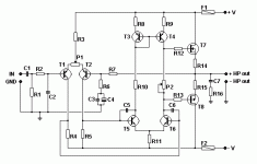
The design shown is using the VAS to drive the FETs directly. I do not like this arrangement since it forces the adoption of big medium power transistors for Q3 to Q7 inclusive. Then these load up the LTP, also not good.
Get a better schematic.
Have a look at Quasi's designs. There are three or more threads covering all the detail of the design and build with a wealth of buider input and a superb web site put up by Quasi.
You did search "quasi", you cannot post without saying "yes".
find a schematic that gives what you need.
The design shown is using the VAS to drive the FETs directly. I do not like this arrangement since it forces the adoption of big medium power transistors for Q3 to Q7 inclusive. Then these load up the LTP, also not good.
Get a better schematic.
Have a look at Quasi's designs. There are three or more threads covering all the detail of the design and build with a wealth of buider input and a superb web site put up by Quasi.
You did search "quasi", you cannot post without saying "yes".
mosfet output
andrewt
thanks,for long i've been searching for quasi design,any comment on quasi's n-mos amp,i just wan't to use my n-channel fets,from surplus shop
andrewt
thanks,for long i've been searching for quasi design,any comment on quasi's n-mos amp,i just wan't to use my n-channel fets,from surplus shop
What more comments do you want? He recommended the design to you. Have a look on the threads by quasi, they are full of information.
What MOSFETs have you got?
What MOSFETs have you got?
quasi comp
hello,
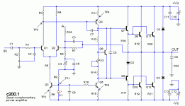
I have tried this output stage, good to me
http://perso.orange.fr/francis.audio2/C07_FB1a.gif
JMB
hello,
I have tried this output stage, good to me
http://perso.orange.fr/francis.audio2/C07_FB1a.gif
JMB
Re: quasi comp
Shouldn't that have at least some sort of thermal sompensation?
jmbaudoin said:hello,
I have tried this output stage, good to me
http://perso.orange.fr/francis.audio2/C07_FB1a.gif
JMB
Shouldn't that have at least some sort of thermal sompensation?
richie00boy said:It uses lateral devices, so no need.
Really? Te top is a 'darlington' with a BJT in front so at best it will have zero Tc at well over 200mA, and the bottom is a CFP with BJT in front which has the TC of the BJT transistor. Have you simulated at different temperatures?
Re: Re: quasi comp
I've read power MOSFETs had negative thermal resistance... so, when, temperature clims up, its conductance goes down, or something like that, but I think that happens with audio output mosfets, the lateral ones, no t teh vertical, made for switching purpose, although you can use it on audio! They're cheaper too!
Thanks to Flavio Dellepiane, visit his site, please.
www.redcircuits.com
ilimzn said:
Shouldn't that have at least some sort of thermal sompensation?
I've read power MOSFETs had negative thermal resistance... so, when, temperature clims up, its conductance goes down, or something like that, but I think that happens with audio output mosfets, the lateral ones, no t teh vertical, made for switching purpose, although you can use it on audio! They're cheaper too!
Thanks to Flavio Dellepiane, visit his site, please.
www.redcircuits.com
In my experience there is no need for thermal compensation with mos-fet bias between 0.3 to 0.7 Amps , thus motorola drivers had their own heather, and Mos where BUZ sort. used with 0.3 °C /W heather per chanel.
Re: Re: Re: quasi comp
Compare Lateral to Vertical FETs and note that lateral change from positive to negative at around 100mA and that vertical change from positive to negative at enormous Amperes Id. They blow up before you can reach the negative coefficient.
Verticals need compensation. Laterals do not need it, but parallel sets do benefit from some feedback by fitting source resistors to each.
Ilimzn was referring to the uncompensated drivers.
yes, go look at the graphs in the datasheets.slideman82 said:I've read power MOSFETs had negative thermal resistance...
Compare Lateral to Vertical FETs and note that lateral change from positive to negative at around 100mA and that vertical change from positive to negative at enormous Amperes Id. They blow up before you can reach the negative coefficient.
Verticals need compensation. Laterals do not need it, but parallel sets do benefit from some feedback by fitting source resistors to each.
Ilimzn was referring to the uncompensated drivers.
Drivers have to dissipate less than 1 Watt with tipical 10 ma. bias so individual U-shaped heatsink can do balance with mos-fet thermal behavior.
The result can be DC offset less than 20mV hot/cold.
JMB
The result can be DC offset less than 20mV hot/cold.
JMB
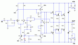
Why don't you build that then? The circuit in your first post is not really suited to easy converting to n-channel mosfet by beginners.
- Status
- Not open for further replies.
- Home
- Amplifiers
- Solid State
- mosfet output conversion