The following circuit appeared in the design ideas section of EDN:
the description can be found here:
http://a330.g.akamai.net/7/330/2540/20050602172840/www.edn.com/contents/images/60905di.pdf
An externally hosted image should be here but it was not working when we last tested it.
the description can be found here:
http://a330.g.akamai.net/7/330/2540/20050602172840/www.edn.com/contents/images/60905di.pdf
Of course - my point was, it's rather strange for a specialised magazine to publish this not noticing such an obvious mistake, let alone in such a simple circuit.
I don't know why Q2 will be killed - I think Q1 has a better chance of getting killed.
The "flaw" in the design is that the voltage drop over Q1 is always Vbe of Q2, and if there is a lot of current going through Q1, it will get hold quickly.
Also, the design would be a lot more interesting if it is done on N-channels.
The "flaw" in the design is that the voltage drop over Q1 is always Vbe of Q2, and if there is a lot of current going through Q1, it will get hold quickly.
Also, the design would be a lot more interesting if it is done on N-channels.
Guys, I'll guess you don't have notice that this mosfet is connected backwards (we use this also at work) and the circuit may not need any gate resistors. This has to be determined from case to case.
Therez no base current limit for Q1..in a practical circuit any short or overload will damage Q1 ......
You may have Vgs breakdown for the kind of voltage solid-state amp will see.
Q2 is fine. It should turn Q1 off fast enough before its base-emitter junction melts.
Q2 is fine. It should turn Q1 off fast enough before its base-emitter junction melts.
peranders said:Guys, I'll guess you don't have notice that this mosfet is connected backwards (we use this also at work)
are you sure about that?
... no, I'll take it back  ... but we still use mosfet's backwards at work for reverse polarity protection.
... but we still use mosfet's backwards at work for reverse polarity protection. tlf9999 said:I don't know why Q2 will be killed - I think Q1 has a better chance of getting killed.
The "flaw" in the design is that the voltage drop over Q1 is always Vbe of Q2, and if there is a lot of current going through Q1, it will get hold quickly.
Also, the design would be a lot more interesting if it is done on N-channels.
Not true on either account.
It's a Pch MOSFET shich means that the resistor R3 (or Rg, difficult to read) will keep the Vgs equal to Vin unless Q2 prevents it. For standard VMOS this implies an absolute maximum Vin of 20V. A zener diode between G and S to limit the Vgs will alow higher input voltages.
Vds will be nigligible as long as Vin is over some 6-7V, because the MOSFET will be working in the Rdson mode, as a very low value resistor. Q2 senses the voltage drop on this resistor and if it approaches 0.7V, turns off the MOSFET. As Vds will then increase (MOSFET goes open), Q2 will continue to keep the MOSFET off unless the current drops to a value where the voltage drop on R1 will become lower than 0.7V.
And here is why Q2 will die, almost instantly, unless it gets a base resistor:
Assume voltage source at input and short at output, for instance an output capacitor - in order for the MOSFET to start conducting, the input voltage should be at least 3V or so, unless a very low threshold MOSFET is used, in which case it can be about 1V. This implies 1-3V across BE of Q2, which pretty much means instant death. R1 must be chosen such that R1 never develops more than 0.7V across it until the input voltage reaches 3-4V, which is a problem without a proper solution - for a short circuit at the output, the input supply would already have to be current limited for this to work, which begs the question why this circuit in the first place.
Even if Q2 survives power-up, when the voltage across the MOSFET reaches 0.7V, R1 would then have to somehow keep it limited to 0.7V for Q2 to survive. Once 0.7V is reached across BE of Q2, the MOSFET is switched off, which removes one path for the output current, and leaves only R1, which means that the voltage across BE of Q2 would start suddenly increasing further (it's a foldback effect), for a short at the output, up to the full Vin can get across BE of Q2. Result: dead Q2.
As for Q1 heating up, since the voltage across it is limited to 0.7V or so, it comes down to chosing the appropriate MOSFET, Pdiss = 0.49/Rdson. This is actually quite easily manageable.
Without adding the missing base resistor to Q2, the operation of the circuit cannot be described properly, so assume it is there. Then the operation of the circuit is as follows:
At switch on of the input voltage, C1 is still discharged. There is a big voltage difference across Q1 (initially the input voltage), which turns on Q2. The base resistor of Q2 limits the base current. Because Q2 conducts, the PMOS is turned off. This leaves R1 as a path to charge C1 slowly. When C1 is almost fully charged, the voltage across Q1 becomes smaller than 0.7V, so Q2 stops conducting. Then the gate of Q1 is pulled to ground by Rg, so Q1 switches on (PMOS) and shorts R1. Now big currents can flow to C1 and the load.
This will work for only small input voltages as ilimzn already said, because Vgs of Q1 is not limited, but adding a zener across gs would solve this limitation. Furthermore the load current should be quite small at power on because Q1 is still off and a big current would cause a too big voltage drop across R1 which keeps Q2 on and Q1 off. So this circuit is not really useful for class A amplifiers, or with a rather small value of R1. R1xIs<0.7V is necessary, with Is the constant power supply current. For class B amplifiers this will work better because the supply current will be small most of the time which allws for C1 to charge, so Q2 will switch off and Q1 will switch on.
Steven
Does this thing actually work in reducing "in-rush" current?
I am not sure as there seems to be 'positive" feedback here. As the voltage on the capacitor gets to a point where the voltage drop off D and S is below Vbe of Q2, Q2 starts to shut off, and the voltage drop off G and S of Q1 goes up, further increasing the voltage on the capacitor. Band! big current rush.
I suspect the sudden turn-on of Q1 isn't desired.
I think it will work (with base resistor for Q2 and zener for Q1, depending on input voltage).
The inrush current at the end of the cycle where C1 is charged the last 0.7V will be small compared to the inrush current that would have been there without the circuit, charging from zero to max.
Steven
The inrush current at the end of the cycle where C1 is charged the last 0.7V will be small compared to the inrush current that would have been there without the circuit, charging from zero to max.
Steven
With the resistor added to the base of Q2, I think it should work as a simple foldback current limiter. However, note that foldback limiting is not practical with non-linear loads like light-bulbs.
Note also that this circuit may fail to start up even with a simple resistor connected to the output due to the non-linear foldback action of the P-ch MOSFET
Note also that this circuit may fail to start up even with a simple resistor connected to the output due to the non-linear foldback action of the P-ch MOSFET
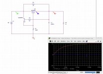
Here is what I have simulated.
It worked, for the most part. There is a graduate charge-up of the capacitor. At just shy of 140ms, however, there is a sudden turn-on of the PMOSFET. And the "in-rush" current through the mosfet is about 7am - not a big deal but I don't think it is as gentle a solution of the author had intended.
Question for everyone: how to solve the problem?
Also, how would the circuit perform when the power is turned off after the capacitor is fully charged?
Attachments
The 140ms depends of course on the value of R2 and C1 in your drawing. The initial peak current will be 5A in this case (through R2, so not visible in your graph). The 7A peak current through the FET will be less in practice, since the C1 will have some esr, and the series resistance of the transformer and rectifier will be even more.
You have the circuit in the simulator, just have a look what would have happened with the inrush current without this limiter. Because the circuit uses an ideal C1 and zero impedance voltage source, the inrush current is easily above 100A.
Switching on the load after C1 is charged will not change much in your case. Your load is just 50mA, but that is already on the edge. If the load is bigger, you have to decrease R2 already.
Steven
I tried a few P-channel MoSFETS and found that the "in-rush" current changes quite significantly with your choice of MOSFETs, from a few hundred ma to close to 10A.
I would venture that slower MOSFETs get lower in-rush current.
I would venture that slower MOSFETs get lower in-rush current.
- Status
- Not open for further replies.
- Home
- Amplifiers
- Solid State
- MOSFET Inrush and Short Circuit Limiter