I have a wide gap in my knowledge of electronics, and this, concerns modelling a transistor's behaviour. While reading, I encountered the Eber's Moll transistor model, specifically, the formula:
I tried to apply this model to the 2N4401 transistor but failed to reconciliate it with the model used by LTSpice.
I am perplexed, because models, are expected to be representative of what they model.
Back when I was still an adolescent, many many years ago, my first serious reading in electronics used the h-parameters and it was very tedious with loads of formulae. What I am reading now, is claiming one does not need h-parameters as there are better models which are easier to apply. The author suggests the Eber's Moll model, as stated before.
Code:
Ic = Is[exp{Veb/(kT/e)} - 1]
Where:
Ic is collector current
Is is saturation current
Veb is the base emitter voltage

k = 1.36e-23 (Bolzmann constant)
T = 293 for room temperature at 20C
e = 1.6e-19 Coulombs.
I tried to apply this model to the 2N4401 transistor but failed to reconciliate it with the model used by LTSpice.
I am perplexed, because models, are expected to be representative of what they model.
Back when I was still an adolescent, many many years ago, my first serious reading in electronics used the h-parameters and it was very tedious with loads of formulae. What I am reading now, is claiming one does not need h-parameters as there are better models which are easier to apply. The author suggests the Eber's Moll model, as stated before.
It's a simple transistor. Make your circuit and observe.
Theoretical results using algorithms and software, is no substitute to knowledge.
Theoretical results using algorithms and software, is no substitute to knowledge.

To Mooly:
While I duly thank you for posting, reading the help page does not offer what I am after. The page discusses subject matter at a far higher level than I can comprehend at this stage. I am after a calculation system/model that enables me to work out transistor behaviour. To give an example, in mechanics, forces are effectively represented by vectors and moments. Vectors are added/subtracted geometrically and moments are the product of force times the perpendicular distance from the centre of turning/fulcrum. I need something similar to this, but for electronics.
While I duly thank you for posting, reading the help page does not offer what I am after. The page discusses subject matter at a far higher level than I can comprehend at this stage. I am after a calculation system/model that enables me to work out transistor behaviour. To give an example, in mechanics, forces are effectively represented by vectors and moments. Vectors are added/subtracted geometrically and moments are the product of force times the perpendicular distance from the centre of turning/fulcrum. I need something similar to this, but for electronics.
I have a wide gap in my knowledge of electronics, and this, concerns modelling a transistor's behaviour. While reading, I encountered the Eber's Moll transistor model, specifically, the formula:
Code:Ic = Is[exp{Veb/(kT/e)} - 1] Where: Ic is collector current Is is saturation current Veb is the base emitter voltage k = 1.36e-23 (Bolzmann constant) T = 293 for room temperature at 20C e = 1.6e-19 Coulombs.
I tried to apply this model to the 2N4401 transistor but failed to reconciliate it with the model used by LTSpice.
What bias conditions did you use for the 2N4401?
The equation applies when the transistor is biased in the forward active region, not in saturation, not in high injection, not in avalanche breakdown and not at such a high current that the resistivity of the base and emitter material plays a role. Besides, it doesn't include the effect of variations in the collector-emitter voltage (Early effect). For a 2N4401, it should be pretty close at collector currents in the 100 uA to 10 mA range and a constant collector-emitter voltage between 1 V and 30 V.
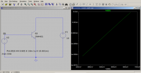
I am not biasing the transistor to exclude further complications as a result of biasing. I am using a voltage source with a constant DC component plus a sawtooth signal and simulating for just one cycle excluding the 1uS fall time. Then, I am plotting V(BE) versus Ic to investigate the transistor behaviour.MarcelvdG said:What bias conditions did you use for the 2N4401?
Since many different semiconductor based circuits are designed continuously, I am assuming, there is a computational methodology which works and is reliable. As I wrote earlier, I was first introduced to the h-parameter system, but the book "The Art of Electronics" is claiming the Ebers Moll model is easier to use, faster and equally precise.
OK, but how do you connect the voltage source to the transistor and in what range are the currents and voltages that LTSpice reports? Can you post a schematic or a Spice netlist?
The equation you posted is very useful, but it has its limitations. The models used by circuit simulators include extra factors and terms for Early effect, saturation, working in reverse, high injection, ohmic resistance of the collector, base and emitter regions. Besides, there are dynamic effects (junction and diffusion capacitances) and noise. The fanciest models also include things like weak avalanche effects, although I don't know if LTSpice supports those. When you want to use a transistor in strong avalanche, all simulator models I know of produce nonsense.
The equation you posted is very useful, but it has its limitations. The models used by circuit simulators include extra factors and terms for Early effect, saturation, working in reverse, high injection, ohmic resistance of the collector, base and emitter regions. Besides, there are dynamic effects (junction and diffusion capacitances) and noise. The fanciest models also include things like weak avalanche effects, although I don't know if LTSpice supports those. When you want to use a transistor in strong avalanche, all simulator models I know of produce nonsense.
Last edited:
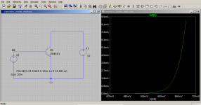
I am posting a screenshot of the schematic and an output graph of Veb VS Ic for Vce = 10V. The circuit is simply a transistor connected in common emitter configuration. No resistors are used in the simulation.MarcelvdG said:OK, but how do you connect the voltage source to the transistor and in what range are the currents and voltages that LTSpice reports? Can you post a schematic or a Spice netlist?
Attachments
What does it look like when you plot the current on a logarithmic scale? Is there a straight part of a few decades? If so, then that part should fit reasonably well to your equation.
Changing the current axis to logarithmic results in a straight line as shown in the attachment.
Added Later to add more information:
Since, the equation of a line is Y = m.x + c, I am tempted to plot V(EB) VS log(Ic) for various transistors under LTSpice to get an idea which Vbe range results in a line. That will give me a clear idea of what to expect from transistors and the Ebers Moll equation.
My preliminary conclusion, till now, is that there is a linear relationship from V(EB) = 0.3V to about 0.75V. Afterwards the relationships departs from linear.
Attachments
Last edited:
That sound quite reasonable, I also see that the slope is close to 1 decade per 60 mV. ln(10) kT/q is approximately 60 mV at room temperature, I'm used to calling the unit charge q rather than e.
Does the lower limit depend on the Gmin setting of the simulator? In real life it depends on crystal defects, in simulation it is often the Gmin limiting it.
Does the lower limit depend on the Gmin setting of the simulator? In real life it depends on crystal defects, in simulation it is often the Gmin limiting it.
I did not change any advanced settings on LTSpice. I did not know I could limit the simulator to assume a minimum of Gmin.MarcelvdG said:Does the lower limit depend on the Gmin setting of the simulator? In real life it depends on crystal defects, in simulation it is often the Gmin limiting it.
I run the simulation for NPN 2SC4717 to try to figure out why the Ebers Moll relation was not working for me. After simulation and plotting log(Ic) VS V(EB) I took two points on the extremes of the linear segment and calculated the line gradient and y-intercept. At the end, I arrived at the following equation:
Ic = 7.51e-14*exp(V(EB)/0.0261)
Please note, I am using volts for V(EB) not millivolts. So, the denominator in the exponent is approximately 25/1000 to compensate for V(EB) being in volts.
The equation shows the Ebers Moll relation works but only for a very limited range of V(EB). My investigations are showing this range is 0.3V to 0.7V. After 0.7V the graph becomes non-linear.
So, my conclusions are:
a) Ebers Moll relation does not apply outside Veb < 0.3V and Veb > 0.7V.
b) Ebers Moll relation is concerned only with small signal analysis/calculation.
c) Large signals require another model.
According to the above, the Ebers Moll relation should, according to my logic, be helpful to analyse VAS stages of amplifiers, but correction for the Early Effect has to be made.
About Distortion of Amplifier Output Transistors:
Plotting Ic VS Veb made me realise, although I may be wrong, that the fact that there is a logarithmic part followed by a non-logarithmic part in the plot may contribute to distortion of output stages. To me, it seems like having two sets of transistors, one set of low signal transistors which work up to a certain instantaneous voltage output, and another more powerful set which is turned on when that voltage level is exceeded. At the end of the logarithmic linearity, the gain drops implying more drive current is absorbed from the driver stage forcing the input stage to use a higher voltage difference. This voltage difference contains the signal itself plus a distortion component, always according to my logic which may be wrong.
Small signal has two different meanings. Small-signal analysis usually means analysis involving signals that are so small that you can approximate the behaviour of whatever you are analysing with first-order Taylor series. Small-signal transistors usually means transistors that can not handle a lot of power.
I guess you mean the second type of small signal, because with n kT/q = 26.1 mV, a 400 mV range of VBE corresponds to a 4 500 000:1 ratio of collector current and a 4 500 000:1 ratio of transconductance. That's much too large a range to do anything useful with first-order Taylor approximations.
In any case, you indeed need extensions to the model when high injection or bulk resistances come into play, as is usually the case with power transistors running near their maximum levels.
Searching online for existing analytical transistor models, I found lecture notes from teaching institutions (.edu) for the Hybrid Pi and T-Model. I will study the theory in an attempt to understand it. I think, I have to give up trying to invent a method for myself, as that can be an issue communicating my results and problems with others, and is often a waste of time.
I know this is an uphill struggle, but the motivation of being empowered with the skill of doing calculations involving real electronics, is exciting, and is something I have been yearning to achieve since my youth days.
I know this is an uphill struggle, but the motivation of being empowered with the skill of doing calculations involving real electronics, is exciting, and is something I have been yearning to achieve since my youth days.
As I know it, the hybrid pi model is a small-signal model in the first of the meanings that I mentioned. It's a linearized model that tells you what happens for small excursions around a bias point. In that sense it is similar to the h parameter models, but it is more physical and less mathematical.
As it's a small-signal model, for its results to be close to reality, the variations in base-emitter voltage have to be << kT/q, the variations in the currents much smaller than their DC values. Dynamic effects are included via the capacitances cpi and cmu.
As it's a small-signal model, for its results to be close to reality, the variations in base-emitter voltage have to be << kT/q, the variations in the currents much smaller than their DC values. Dynamic effects are included via the capacitances cpi and cmu.
Last edited:
- Home
- General Interest
- Everything Else
- Modelling a transistor's behaviour.