Generally and precisely
- the feedback factor k = RN/ (RF+RN), sometimes also called kü in German
- the voltage gain of the closed loop is calculated as Vuo / (k*Vuo + k); simplified a little because we are basically talking about approximations.
For a better overview:
A = OLG / (OLG + 1)
B = (RF / RN) + 1 ---> 1/k
CLG = A * B
The larger Vuo or OLG becomes, the more likely term A becomes practically 1. With almost 80dB equal to 10000, this results in 0.999... for A. Gain thus always approaches to be B.
Greethings,
HBt.
(Possible mistakes are due to a sleepless night, for which I apologize.)
Conclusion:
Minor changes to the OLG do not change the quasi One of Term A! That's one of the great things about negative feedback systems. But another thing I ask myself is what abbreviations and terms should I (must I) use so that I can make myself understood correctly in an international forum?
As you can see immediately, the change from 220kOhm to 100kOhm can have no (great) effect in context. Although the ratio 10 / 22 is quite considerable, it does not take into account the load (pressed out by rbe2). rbe2 is considerably smaller than RC1.
The entire open loop is practically calculated as
[( S1 * RC1||rbe2 ) * S2 * RC2] / [( S1 * RE1 +1 )]
with
S = beta/rbe. See above, posting #34.
But the design issue is not quite that simple, because both the feedback network loads the output of the entire amplifier and the input resistance of subsequent circuits.
[( S1 * RC1||rbe2 ) * S2 * RC2||LOAD] / [( S1 * RE1 +1 )]
However, since the negative feedback not only has a positive influence on the stabilization of the amplification factor, but also on the dynamic input and output resistances, we set RL equal to infinity. There is therefore no further load on the collector circuit of the second stage - and now we ignore the LOAD variable.
|Z_in| approaches rbe1 + Vuo * rbe1 and |Z_out| approaches RC2 / (Vuo +1). We are currently still ignoring rce in the analysis, the question is, can we do this? Dynamically, there is again a parallel connection in our equivalent concept, ra = rce2*RC2 / (RC2 + rce2). Considered on its own, this means 10kOhm||30.43kOhm = 7.53kOhm.
The deeper we delve into the entire AC equivalent circuit diagram, the system, the more interesting it becomes - thumb rules and overrides no longer help, it becomes more challenging when the local and global loops are closed.
Have fun with it.
With all the nice simplifications, we also assume that rce is much larger than RC, but with almost 30kOhm (at the operating point) this is not the case at all and RE must also be transformed to the other side ...
Sometimes things get really complicated and models become increasingly inadequate the deeper you look into the circuit - even with a two-stage circuit with BJTs. The parameter dependencies and the feedback (and the frequencyband) finally makes our DIY brain go into overdrive.
The recommendation can only be' to learn the business from scratch (and to practice, practice and practice again) or to use a computer-aided simulation program (as a schematic). Trial and error, supported by measurements, would be another viable alternative.
Addendum
If I take all resistors into account with my model transistor (including R17+R19 as load) then Vuo_220k is just 73.38dB and Vuo_100k just 73.17dB.
This means that the calculation with paper and pencil even confirms the OLG from my original simulation. No wonder, because the BJT is the same. The roughly and intuitively determined 78.44dB is correct as follows 73.38dB.
Last edited:
Let's do it from scratch
Model parameters of a Siemens BC 5xx Typ:
rce= 30k43Ohm
beta= 346
rbe= 4k85Ohm
D= 212*10^-4
Expressed as h-parameter of the four-pole:
h2_2= 1/rce
h2_1= beta
h1_1= rbe
h1_2= D
Normally, it would be extremely important to have the exact characteristics of the transistor available for the actual recipe; it makes sense to transfer them into a so-called 4-quadrant field (with linear divisions) - this way you get to know the LF transistor quite well. But we want to examine an existing circuit, so let's dispense with this elementary first step, the recording of the characteristic curve. In the second step, we would determine the optimum operating point. We also have the option of using graphical solution methods.
1)
We consider the last stage first, open the feedback loop and set a load on the collector (circuit output):
V2 = Tr2 => model transistor
RC2 = R9 => 10kOhm
RE2 = R11_15 => ac-shorted
RF = R17_19 => (220k+22k)
RL = Rload => input resistance of our preamplifier 10kOhm
Au2 = Gain
Ra = RC2 || (RF || RL) = 4899Ohm
Now we calculate the resulting voltage gain of the stage:
Au2 = - (h21 * Ra) / (h11 + delta_h * Ra)
Au2 = beta * 4k899Ohm / ((rbe + (rbe/rce - beta*D) * 4k899Ohm)
It is now questionable whether we can use rbe if the dynamic output resistance of the first stage is in parallel to the base-emitter path.
rbe´ = (beta*RE1 + rce) || RC1 || rbe
with
RE1 = R7 = 330Ohm
RC1 = R5 = 220kOhm (percy changed to 100kOhm)
rbe´ = 4k592Ohm
Au2 = 346 * 4899 [V/A] / 4971 [V/A] = 341.4
OLG is now calculated as 50.66dB with typical preamplifier load and also RF as additional load -> the voltage gain of the loaded, simple emitter circuit of the bipolar NPN or PNP transistor.
2)
Now we are missing just under 30dB of the first stage to achieve a really sufficient core amplification of 80dB.
In the next step we allow ourselves to set Ra = rbe' from the 1st step above and now determine rbe' with rbe || RB1, with RB1=R14.
rbe' = 1/( 1/4847Ohm +1/220kOhm) = 4k742Ohm
Next, we allow ourselves to use a simplification for the time being and consider RE1 as short-circuited, which is of course not allowed - but let's see what comes out and decide at the end whether we were allowed to simplify.
S = beta / rbe'
Au1 = S * Ra
= 73.1mS * 4k592Ohm = 335.5 -> (50.51dB)
k = RE1 / (RC1 || rbe)
= 330Ohm / 4k742Ohm = 69.6*10^-3
Au1´ = Au1 / (1 + k*Au1) = 335.5 / 24.4
= 13.78
OLG is now calculated!
22.8dB (+ 50.66dB) = 73.46 dB
V1 = Tr1 => model transistor
source resistance => 0 Ohm (ac-view).
Last edited:
2.1)
Let us briefly neglect the load of the first stage and consider it alone. RB1 = R14 = 220kOhm is considerably greater than rbe we will also ignore it.
S = beta / rbe = 71.5mS
k = RE1 / RC1 = 0.0015
Au = (S * RC1) / (1 + k * S * RC1)
with
RC1 = 220 kOhm -> 639.6 -> 56.12dB
RC1 = 100 kOhm -> 609.8 -> 55.70dB
2.2)
Now we load the source with our second stage and the value of rbe.
r_source = ra
ra = ((beta * RE1) + rce) || RC1
ra_a = 144k744Ohm || 220kOhm = 87k304Ohm
ra_b = 144k744Ohm || 100kOhm = 59k141Ohm
a_a = 20*log[rbe / (rbe + ra_a)] = -25.6dB
a_b = 20*log[rbe / (rbe + ra_b)] = -22.4dB
Au1(RC) = 56.12dB - 25.6dB = 30.52dB
alternativ
Au1(RC) = 55.70dB - 22.4dB = 33.30dB
Now you can see the originally assumed gain expressed as just under +3dB.

2.3)
The same procedure with the second stage.
Au = S * RC2 = 714.7 -> 57.08dB
ra = rce || RC2 = 7k527Ohm
Rload = RF || re_preamp = 1/(1/242kOhm +1/10kOhm) = 9k603Ohm
a = 20*log[Rload/ (Rload + ra)] = -5.03dB
Au2(Rload) = 57.08dB - 5.03dB = 52.05dB
If we now add up, we get exactly what we want, namely greater than 80dB gain -> now we could theoretically design the RIAA network without correcting the time constants, if we could still assume an ideal source at the same time.
Finally, the prize question remains: who will find the error and be able to correct it?
😉
2.3.1)
Unfortunately, RC2 is not sufficiently larger than rce and therefore we are not allowed to simplify and work with the approximation.
At this point we have to use S * ra and minus "a" let us get = 49.6dB.
2.1.1)
The same applies here and we end up with (48.1dB - 25.6dB) = 22.5dB
2.4)
OLG with this permitted method is actually 49.6dB + 22.5dB = 72.1dB
A = 3589 / 3590 = 0.99972145
B = 242kOhm / 330Ohm +1 = 734.333
close loop gain is now for very low frequencys 57.32dB; unfortunately, we do not couple back a voltage, but a current at the emitter of the V1 - the emitter as a negative input, that already suggests the next inattention!
EXIT at this point
That was the long answer to your question @percy. And the frequency-dependent behavior of the entire two-stage circuit is still missing, as well as the combination with the RIAA network.
Looking ahead, it would be interesting to move on to synthesis and dimension a simple equalizer preamplifier step by step - with justifications, of course.
I don't want to take on this task at the moment, as there are already countless examples available. I think you can already see that the successful dimensioning of a two transistor EQ is actually not an easy task - the surface has been scratched.
Best wishes and have fun with the stony road, it's a little bit hardcore
HBt.
😉
Last edited:
Unfortunately, RC2 is not sufficiently larger than rce and therefore we are not allowed to simplify and work with the approximation.
Unfortunately, rce is not sufficiently larger than RC2 and therefore we are not allowed to simplify and work with the approximation.
Requirement is:
RC greatly smaller then rce
RC <<< rce
or
rce >>> RC.
I have once again determined the influence of R5=RC1 without simplifications and approximations (with correct transformation) on the open loop gain. Everything calculated by hand.
Au1(220kOhm) = 22.4dB
Au1(100kOhm) = 22.2dB
As a circuit improvement, the static consideration (dc-view) and thus the dimensioning of the operating points in advance is the most important criterion. We need to know the movement of the operating point on the dynamic working line and determine it wisely, both of which Percy is now trying to optimize afterwards.
Basically, it is wise to sketch the resulting network, to know the h-parameters and to use the PI equivalent circuit diagram for the LF range and not to overuse the usual approximations and simplifications.
For static testing, I would measure at least all potentials with a high-impedance DVM, but also VBE1, VCE1, VBE2, VCE2!
Incidentally, you can keep in mind that without current feedback and current injection, the THD would already be in the percentage range due to the input BJT (and his nature) in the emitter circuit alone.
My quick draft in posting #18 shows how significantly the static design can differ.
Last edited:
hbtaudio / Percy, I added the 1nF at the end , and also put in C03/C05 from the original Realistic
schematic, which can be populated only if needed.
schematic, which can be populated only if needed.
Attachments
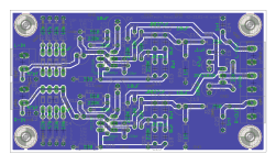
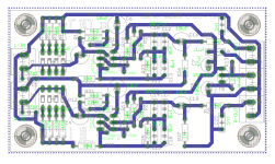
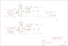
C20, C21, C22, C23 have no place on the PCB, they are counterproductive - also the Input DIP-switch selection!
Do us a favor: please remove my name from the board and the drawing, instead refer to the forum "www.diyaudio.com" - if there are commercial intentions, consider the warranty... etc.pp.
C20, C21, C22, C23 have no place on the PCB, they are counterproductive - also the Input DIP-switch selection!
Noted the feedback - thanks - will address next weekend I am free.
Disclaimer to all - the files I posted were made for my own learning, untested, for diy use.
Hello
@quadtech
We haven't heard from you for a long time. I hope you have already been able to put both classic designs into practice.
I would be pleased if you could write a few sentences about the equalizers and also publish a motivating photo of the circuit boards.
All the best and greetings,
HBt.
@quadtech
We haven't heard from you for a long time. I hope you have already been able to put both classic designs into practice.
I would be pleased if you could write a few sentences about the equalizers and also publish a motivating photo of the circuit boards.
All the best and greetings,
HBt.
- Home
- Source & Line
- Analogue Source
- Modding (rebiasing) a 2-stage phono pre