NUTTTR said:
Excellent i'm glad it was my thought too 🙂 I've got to look at that and make sure everything is right in it, bigger caps are on the books so to speak 🙂 Is there anywhere over there (assuming US?) that i can get bigger caps, no one in Aus really specialises in that and when they do they charge stupid amounts for them!
Thanks 🙂
Aaron
Here for example :
http://www.schuro.de/preisl-bc154.htm
but there are also Elna LPO , Epcos Sikorel ...
alain
An externally hosted image should be here but it was not working when we last tested it.
Looking at that there, i've (so far) come to the conclusion (maybe wrong) that the D669 screwed to the heatsink (only chip on it's own) is in fact there in relation to the bias in some way - there is supposed to be resistors mounted where the direct wires are - leading me to believe that potentially if i was to add some form of bias adjustment that'd be where it goes - as for what resistance, etc i don't know....
But if i was adding anything, it looks like that's where it should go to me...
I'm actually struggling to find info on biasing, etc, there's plenty of "how do i set it" but things like what i'm (trying) going to do actually isn't done from what i can tell?
If someone else looks at that photo and i'm totally off track (or completely wrong) don't hesitate to yell and scream 🙂
Thanks heaps
Aaron
I think you're right. That looks like a potential bias thingy to me 🙂 You are right, there's very little info around how to design a Vbe mulitplier properly. There's tons of amp circuits and how-to guides floating around, but they all seem to neglect the bias generator. I think the vast majority of bias generators that people use on their own amps are just ripped off other designs, or parts bin 'they'll do' values.
Thing is, the voltage a Vbe multiplier generates is dependent to an extent on the current available to it, so component values are IMO quite important. It's also easy to just slap one together that 'works', but another thing to make one that has a decent and even amount of variation/linearity.
Thing is, the voltage a Vbe multiplier generates is dependent to an extent on the current available to it, so component values are IMO quite important. It's also easy to just slap one together that 'works', but another thing to make one that has a decent and even amount of variation/linearity.
Speaking of bias, I'll bet the TO-126 bolted to the heatsink is the Vbe multiplier. You can reade the bias voltage between the emitter and collector. You should get the same value between the bases of the thre two driver ("in between") transistors as well. I don't see a trim pot, however so there is no way to adjust it. In principal you don't need one except that the (diode like) voltage drop between the base and emitter can vary slightly from unit to unit.
I would guess the configuration is an EF output rather than CFB, but you ought to be able to work that out by tracing what connects to what from the drivers to the output devices. There is a different optimal bias voltage in each case. (~2.89V for EF and 1.28V for CFB are typical) for If you can determine the bias voltage as described above, report it back here and that may provide additional commontary.
I would guess the configuration is an EF output rather than CFB, but you ought to be able to work that out by tracing what connects to what from the drivers to the output devices. There is a different optimal bias voltage in each case. (~2.89V for EF and 1.28V for CFB are typical) for If you can determine the bias voltage as described above, report it back here and that may provide additional commontary.
get the schematics or better yet service manual
...if you can, really I mean it. The size of the power supply is such that a wrong adjustment, or a slip with a probe will make a big bang, wipe out a nice collection of transistors and induce a lot of swearing.
The ne5532s on the peripheral board are almost certainly mic amps, probably used to do balanced to unbalanced conversion. Lose them if you don't need them. If you don't use them they only add a little noise, but there is always the chance of other stuff being picked up too
Adjustment of bias is easy, but if you don't have a variac you run the risk of the whole amp going poof as you turn it on. I just bought and fixed 2 amps from a guy that started modding without the schematic. They were less half the power of yours, but it still destroyed half the outputs, all the drivers, VBE circuitry, burned tracks on the board, it was not a pretty sight. I could still here the echoes of the cursing as I took the cover off...he'd replaced a 2.2k resistor with 22k.
If you 'must' do this without the schematic, build a test rig, get and install a much smaller transformer of the same voltage rating, use fuses of 1/10 the nominal value and be really, really careful. There are voltages, on the circuitry side, as well as the mains side that will kill you.
Stuart
more...
As far as I can see there is no bias pot, no big deal, but it means the vbe multiplier was loaded with a pair of resistors set for the cumulative gain and VBE of the outputs and drivers. Once you find the correct pair of resistors, you can change just one and control the bias in easily calculated increments. But you'd probably want to replace the fixed resistor with a pot to do in situ adjustments, then measure and replace the pot.
You should be measuring bias with the amp disconnected from anything, from the outside pair of leads of the 3 legged emitter resistors. Each transistor 'should' be identical in this respect, and I'd expect to see a few 10's of millivolts across the pair of resistors, indicating a few 10's of milliamps for each output. With voltage rails as high as you have there is no real way to set the bias high, the output will cook itself, each amp through the outputs corresponds to over a hundred watts of dissipation.
The zeners are probably there to provide a regulated supply for the front and ne5532's. The fact that they aren't dont seem to be working right, might be a big problem.
Stuart
Wiring seems very poor from these pictures. Never put signal wires and power wires together. Twist +Vcc and -Vcc, etc...
There are huge radiating loops in this wiring. +Vcc, -Vcc and PCB power grouns should travel together with the output wire from the PCB to the central ground, then, the output wire and the ground wire [taken from the star ground] should travel together to the output binding posts, everything twisted
Also, this circuit is probably class B like many other cheap PA amps, so it has no provision for bias adjustment, It doesn't even appear to have a Vbe multiplier [almost mandatory for class AB]
If, in fact, the NE5532s are part of a "balanced line reciever" it may be possible to replace the whole mess with one SSM2141 or INA134 for each channel. These are specificly designed for the purpose and (per the datasheet) have noise and distortion figure way, way below any opamp. They would also take up less space.
Regarding the routing of the signal wiring too close to the power supply: if the physical limitations of the layout don't alllow you to put enough space between them and noise sources, you might try shielded wiring of some kind where one end of the shield mesh/foil is connected to ground. This kind of cable tends to be stiff and difficult to work with, but not impossible.
Regarding the routing of the signal wiring too close to the power supply: if the physical limitations of the layout don't alllow you to put enough space between them and noise sources, you might try shielded wiring of some kind where one end of the shield mesh/foil is connected to ground. This kind of cable tends to be stiff and difficult to work with, but not impossible.
I mentioned the maximum dissipation being 3000 watt , from 20 devices.
Maximum dissipation is NOT maximum power level.
Nutttr mentioned 78 volts from the powersupply.
Maximum dissipation occurs at 50% of the maximum output signal, 39 volts.
As a single channel should deliver its power in 2 ohm, the load being 4 ohm in bridged mode, the dissipation becomes :
(39 *39)/2= 760.50 watts.
These 760.5 watts need to be divided by 10 transistors, 76.5 watts each.
As the temperaturegradient is measured from 25 to 150 degrees ambient the thermal resistance is 125/150 = Rjc=0.83.
The thermal resistance from the transistor to the heatsink is something like 0.50
With the proper heatsink and enough air flowing over it from a vent it is possible to reach 0.05 for the heatsink.
I am sure someone here can tell you where to download a sheet with which to estimate the cooling factor of a given heatsink.
I have graphs that give thermal resistance for different airflowspeeds for different static heatsink thermal resistance factors.
Each transistor sees 1/10 of the heatsink, for one transistor the thermal resistance becomes 10 * 0.05= 0.50.
Total thermal resistance for one transistor is :
0.83 + 0.50 + 0.50 ~ 1.8
With a given 125 degrees above ambient temperature(25) each device is capable of dissipating nearly 70 watts (125/1.8) before it breaks down.
For 10 output devices this becomes 700watts.
If the top potential reaches 78 volts the amp will die as 760.5 watts is needed at 2 ohm( presuming the protection circuit that limits output current is removed).
In reality the voltage level will drop under load, it will be lower than 78 volts, if it is lower than 74.8 volts the output transistors will live.
Furthermore, as the amp is not intended for full force PA apllications the average dissipation is a lot lower than the figure mentioned.
With an added transformer and more electrolytics the voltage would be more stable and the power stored in the powersupply would be sufficient to kill the output section.
I think i saw thermal protection on the heatsinks, with fuses in the supply lines the amplifier would have sufficient protection.
sam9 :
Shields do little against magnetic fields, they only prevent electric fields from affecting high impedance circuits
Shields do little against magnetic fields, they only prevent electric fields from affecting high impedance circuits
Thanks all 🙂 Been a great help!
Stuart - i am trying to get one, but haven't had much success yet, i've found a contact in aus who may be able to get one... It is VERY VERY much like the P69 sub amp on the previous link someone gave me! very much!
Before powering up the amp (i'm only doing 1 channel at this stage, then the other one once i work it out 🙂) i'd make sure the vari-resistor will be at 0ohm, or matching whatever resistor is there - at this stage it's a wire link i'm assuming will have to go and vari added... I got a bit of an image that i took and drew up the schematic a little so everyone get's an idea of what's going on....
As for the wiring, that's definately got to be done... however there is no noise at all through the amp, it's very very quiet and being class b wiring doesn't seem to affect the sound quality, it may be a problem if i can get it into class a/b but we'll see 🙂
As for the power supply, it does lose quite a bit of power when cranking it... a lot... I think i should do the caps alone maybe and maybe go a bigger transformer, still not sure what i'll end up doing yet as i'm more interested in moving away from class b now!!!
The voltage between the emittor and collector is 2.028v (dc obviously!).... Given the above picture, is there a chance anyone can tell me exactly what's working where?? Thanks very muchly!
Aaron
Stuart - i am trying to get one, but haven't had much success yet, i've found a contact in aus who may be able to get one... It is VERY VERY much like the P69 sub amp on the previous link someone gave me! very much!
Before powering up the amp (i'm only doing 1 channel at this stage, then the other one once i work it out 🙂) i'd make sure the vari-resistor will be at 0ohm, or matching whatever resistor is there - at this stage it's a wire link i'm assuming will have to go and vari added... I got a bit of an image that i took and drew up the schematic a little so everyone get's an idea of what's going on....
An externally hosted image should be here but it was not working when we last tested it.
As for the wiring, that's definately got to be done... however there is no noise at all through the amp, it's very very quiet and being class b wiring doesn't seem to affect the sound quality, it may be a problem if i can get it into class a/b but we'll see 🙂
As for the power supply, it does lose quite a bit of power when cranking it... a lot... I think i should do the caps alone maybe and maybe go a bigger transformer, still not sure what i'll end up doing yet as i'm more interested in moving away from class b now!!!
The voltage between the emittor and collector is 2.028v (dc obviously!).... Given the above picture, is there a chance anyone can tell me exactly what's working where?? Thanks very muchly!
Aaron
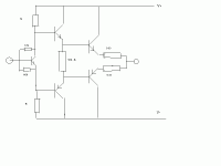
a typical vbe multiplier...
is just three components, a pair of resistors from the collector to the base and the base to the emitter of the bias control transistor.
The nature of silicon transistors is such that approx. 0.6v will appear across the base emitter resistor, and the current to achieve that has to flow through the resistor coming from the collector to the base. So the voltage from the collector to the emitter will be 0.6v * Rcb/Rbe. In a normal darlington complimentary output stage this will be approx 2.0-2.2v (giving 0.5-0.55v forward bias each to the drivers and outputs), so if Rbe were 600ohms, then Rce would be approx. 1.6k. Obviously these values are arbitrary on my part, but the key is the ratio, and the minimum current needed to ensure proper bias of the outputs.
I have attached an incredibly crude drawing I did, it shows the relative positions of the typical components. On your board there are a couple of little transistors that could be part of a protection circuit, of perhaps you have a triple darlington output, in which case you'd want 3.1-3.5v bias from the multiplier, and the upper resistor would be approx. 2.5k.
The value of the upper resister is the one I change, lower is safer and it will never be higher than the value required to forward bias the drivers and outputs, once you get to a certain point, very small changes in resistor make a big difference to the output stage current. You don't want more than approx. 0.5-0.6v for each of the base-emitter junctions in the output circuit, if you are in any doubt remove the output transistors. If the resistor in the middle is present you will still be able to check the bias voltage before reconnecting the outputs, if it is not present put it in, 500-1k, 2-3 watt should do...
If you decide to install a variable resistor, put it in as the bottom resistor, in series with the 600ohms. If it ever goes open circuit then things fail safe, idle current drops to 0. If it were in the top position and went open, baby go boom...
After installing the control resistors you will need to measure the voltage dropped across the emitter resistors of the output stages, if it is much more than 25-50mv, you need to lower the top resister. Keep a close eye on temp, idle current etc when you first turn it on.
I can't give you more precise values, basically because it depends on individual transistors. I've found modern motorola TO3s require about 0.1v more Vbe than 26 year old Toshibas...
If I were in Australia I'd pop over and help, I love this stuff...
Stuart
Attachments
http://nutter.caraudioaustralia.com/other/DSC01941.JPG
Also was just going to add in that picture the "resistors" on the bottom that link pretty much directly to the D669 are as follows
100ohm - 0ohm (wire link) - 1kohm - 430ohm
"above" that (closer to the top of your screen!)
is 100ohm - 0ohm (wire link)
Also was just going to add in that picture the "resistors" on the bottom that link pretty much directly to the D669 are as follows
100ohm - 0ohm (wire link) - 1kohm - 430ohm
"above" that (closer to the top of your screen!)
is 100ohm - 0ohm (wire link)
Maybe i am in error again:
On the pictures i see emitter resistances but no gate R's.
Supposing the amp needs to be stable when bridged i would think adding a resistor between the gate of each output transistor and the emitter of the driver Q's could be an improvement.
The 2 transistors, a number of resistors and a diode between the drivers make a protection circuit to limit output current.
It has an effect on sound quality , but if you wish to toss out 17.5 amps continuously in bridged mode i'd leave it there.
Vbe Multipler
Earlier in this thread, someone wrote that they could find little/no info on how a Vbe multiplier works, The attached file (unzip to get the Word .doc file) is from some course material at Drexel. The principle is fairly simple. The only difficulty is that in real the BE voltage varries device-to-device from the "ideal" 0.7V.
Earlier in this thread, someone wrote that they could find little/no info on how a Vbe multiplier works, The attached file (unzip to get the Word .doc file) is from some course material at Drexel. The principle is fairly simple. The only difficulty is that in real the BE voltage varries device-to-device from the "ideal" 0.7V.
Attachments
This looks a little like the Prosound amp that is available in the UK. It is supposably 1000W but closer inspection of the spec reveals that to be "music power". Is it nasty all through the frequency/power range.
The other thing I have to say is that in the Peavey 8.5C manual says that it too will bridge to do 1100W but it is for speech. The inference being the PSU and heat disipation can't cope with it for anything other than short bursts. The Prosound forum (no relation) did a shoot-out day and concluded that nothing what more likely to send an amp home in a bodybag than cheap PSUs
Cheap amplifier manufacturers tend to be a little "positive" about their specs. I would be a little worried about what that clip does to the speakers.
Since youre it to overkill, Why not Biamp and run BOTH amps in stereo mode, well within their capabilities?
Home stereo.......... How big IS your home?
Attachments

Thanks for the info so far guys!! It's great 🙂
I'm gonna try fiddling sunday so should be right with some feedback then - see how i go 🙂
Yeah the peavey doesn't make it's bridged output, but that's ok, i use it for my front speakers they dont really need that much power 🙂
The sub amp is the one i'm trying to mod, because it doesn't sound the greatest, i was hoping to do something about that... Power output (or more of it) would be excellent however if it comes down to being class a/b and that's all i can do, that's even better! 🙂
Thanks for the info on the VBE multiplier!
Aaron
bias is...
Aaron,
From your resistor values your amp is definitely biased, ie not class B per se, but possibly underbiased. You should be able to measure about (0.6 * 1k+430/430), approx 2v across the emitter and collector of the 2sd699. Given there are at least 4 base-emitter junctions to forward bias, that is probably on the low side, but it is close. If you measure the voltage across the d699 and don't see 2v, something is broken, for instance it could be the transistor itself is a collector-emitter dead short. You can measure it's C-E resistance with a multimeter, but turn off the amp first.
If any of the protection circuits are broken or miscalibrated it will make the amp sound horrible, they could be clamping early or simply dumping the bias for one pole of the outputs. When properly biased each driver and output should have the standard 0.5-0.6 volts from base to emitter, much more will cook the outputs, less will sound nasty.
Good luck
Stuart
Hi Stuart!
Thanks very much for your help so far, it's excellent!!
Across the D669 is about 2.02v or so...
I've measured across the B-E of the outputs, the C5200's have 0.380v across the B-E the A1943's have 0.502v.... I've tested the (what we assume is!) currently limit transistors, only the collector has about 0.900v on it at idle as determined by the diode's to it... So it would APPEAR to me that they are not on what so ever as no other pins have any power (this may change once turned up though i guess!)
It would seem wierd that if it does have bias, that i'm measuring those amounts across the output transistors and that the value is different (wierd!) for either side.....and then i measure nothing at all across the emittor resistors (big white ones, just in case i'm going mad 🙂) at all!!
Any ideas? At idle i'd assume there's something wrong if bias is different on either side... Bias starts lower too i think and goes up with time and i'd assume it would go up when the amp gets HOT (too late to test this!! 🙂)
Thanks heaps
Aaron
- Status
- Not open for further replies.
- Home
- Amplifiers
- Solid State
- Modding a high power amp...