Hi,
This is the idea I came up while trying to increase the open loop gain of the F5 amp to have a higher more "load invariant" close loop gain (26 dB) . This is really only a mix of a GB-150 (Greg Ball "Amplifierguru") and Pass F5 amp topology. Also, I need a higher power so I plan to use it in class AB mode (about 10W class A and up to about 70W or so in class B) so I save a bit of money on my energy bill and the size of the case which has to pass the WAF...
The C25-C26 caps are bootstrap caps that could be included or not using a switch for audio comparison purpose.
Can you comment on any aspect of this design giving recommendations before I give it a try.... or not...🙁
Thanks
Attachments
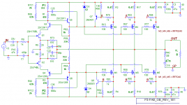
I don't know if NTC1 and NTC2 would be sufficient to prevent thermal runaway in output MOSFETs - you plan to run the amp in AB class, it's quite different scenario compared to F5
I'd rather go for Vgs multiplier for ensuring thermal stability.
I'd rather go for Vgs multiplier for ensuring thermal stability.
juma said:I don't know if NTC1 and NTC2 would be sufficient to prevent thermal runaway in output MOSFETs - you plan to run the amp in AB class, it's quite different scenario compared to F5
I'd rather go for Vgs multiplier for ensuring thermal stability.
This a valuable comment. I have never used IRFPxxx devices before. I have used IRF340 before (both in class A and class AB)which are also vertical mosfet devices but different than IRFPxxx devices.
Where would you put the VGS multiplier in this design?
Does someone knows how is done the temperature compensation in the "SKA" amp (GB150)?

darkfenriz said:I don't know for sure but probably manipulating tail current of long tail pairs
You mean in SKA amp because I do not have a long tail pair...

In my schematic, would that be similar to use a NTC like I have shown?
AFAIK, SKA uses Lateral MOSFETs (BUZ 9xx) so the temp. comp. is not needed.
You should put Vgs multiplier between the emitters of Q5 and Q6 in you schematic. SEARCH button is your friend 😉
You should put Vgs multiplier between the emitters of Q5 and Q6 in you schematic. SEARCH button is your friend 😉
They are IRF type FETs, and the Vgs are matched within 10mV. Photo shows a pair of TO-92 devices attached to the heatsink for thermal tracking.
http://www.ska-audio.com/diy/Components/300x200_150d.jpg
http://www.ska-audio.com/diy/Components/300x200_150d.jpg
Yes, you are right, the picture clearly shows temp. comp. transistors and IRF MOSFETS. I was seduced by old pictures showing BUZ9xx devices.
I guess you could use Q5 and Q6 for temperature compensation as they are in mosfets gate-source circuit but you have to experiment with R62/64 and R59/60.
Temp compensation
I think that using a VGS there would make the vce of Q5 and Q6 dependent of power supply voltage variations therefore giving output IRF Vertical Mosfet VGS variation too.. .
I try to always use the SEARCH button (I even looked at the SKA forum too) even more than you this time... 😉
😉
That seems a very good idea since the VCE of the BJT decreases with temperature rising per the datasheet. Is that really how the SKA temp compensation is done?
Do you mean that the Ic of Q5 and Q6 changes the vbe relation with temperature?
:
Thanks to all
juma said:...
You should put Vgs multiplier between the emitters of Q5 and Q6 in you schematic. SEARCH button is your friend 😉
I think that using a VGS there would make the vce of Q5 and Q6 dependent of power supply voltage variations therefore giving output IRF Vertical Mosfet VGS variation too.. .
I try to always use the SEARCH button (I even looked at the SKA forum too) even more than you this time...
😉 bogdan_borko said:I guess you could use Q5 and Q6 for temperature compensation as they are in mosfets gate-source circuit but you have to experiment with R62/64 and R59/60.
That seems a very good idea since the VCE of the BJT decreases with temperature rising per the datasheet. Is that really how the SKA temp compensation is done?
Do you mean that the Ic of Q5 and Q6 changes the vbe relation with temperature?
:Thanks to all


All those methods seem OK for preventing thermal runaway, but if you want to keep idle current constant throughout wide range of temperatures, than do build a prototype and check if out.
Experiment is the only way here. Tip: use a hairdryer 😉
Experiment is the only way here. Tip: use a hairdryer 😉
darkfenriz said:All those methods seem OK for preventing thermal runaway, but if you want to keep idle current constant throughout wide range of temperatures, than do build a prototype and check if out.
Experiment is the only way here. Tip: use a hairdryer 😉
ok but my hair do not need a hairdryer anymore...
I prefer to put aload with a high input sinus to increase the temperature during bias adjustment...I am not too concerned about the ambient temperature change in my home...
So except the temperature compensation adjustment to be tweaked is there any other improvement to be done on the design and choice of components before trying a prototype (which could take a few since I have to get IRFP devices and heatsinks ...)?
with "curent displacer"...
Hi
I have added a "current displacer" at output of amp (refer to circuit at right of D1 and D2)
Question: Should M7 be the same type (VMOSFET) as the other output transistors for optimum performance?
Any other comments?
Thanks
Hi
I have added a "current displacer" at output of amp (refer to circuit at right of D1 and D2)
Question: Should M7 be the same type (VMOSFET) as the other output transistors for optimum performance?
Any other comments?
Thanks
Attachments
It all looks fine to me. Go build that.
What are the figures you got from simulation (THD, SR, bandwidth)?
Regards,
Adam
What are the figures you got from simulation (THD, SR, bandwidth)?
Regards,
Adam
darkfenriz said:It all looks fine to me. Go build that.
What are the figures you got from simulation (THD, SR, bandwidth)?
Regards,
Adam
Thanks darkfenriz !
Unfortunately, parts for that amp will arrive slowly. The chassis with heatsinks will arrive at end of October from Italia ( it has to be good looking for the WAF.... 😉
I need the heatsinks for the initial testing.
I am doing the layout of the pcb.
My simulator does not have THD but anyway I do not rely on sim for that and lower than about 0,01% is good enough for me. I expect this one to be in this order of magnitude since open loop gain with bootstrap caps is about 56 db based on sims.
SR based on sims is incredibly fast probably because of current feedback ... (and no VAS also maybe?...🙄 )
Bandwidth is mainly limited by input cap but without it is more than 1 MHz.
But all these figures are based on "generic" model of transistors and not the real ones...😱
This is the latest update, please comment...
I know I'm just being a wisea$$ , but this amp would look
like a


Rejoyce time...
..but I like LEDs for good voltage reference and low noise...😀
I wanted to use TL431 but at 20-25 ma and 11v...
I am hoping it can play well... and not only
  songs... 😉
ostripper said:
I know I'm just being a wisea$$ , but this amp would look
like a
..but I like LEDs for good voltage reference and low noise...😀
I wanted to use TL431 but at 20-25 ma and 11v...
I am hoping it can play well...
and not only songs... 😉LED's are more thermally stable than diodes anyway,
also a confirmation of proper operation.
Maybe I just have a LED fetish..
As far as heatsinks, I use what is available.
For most amps I order socket A PC heatsinks (4US$ each), line em' up
screw them together , get super .1C/W good looking thermal solutions for next to nothing..(wife won't let me spend alot on DIY)
cheers,
OS
- Status
- Not open for further replies.
- Home
- Amplifiers
- Solid State
- Mix of GB and F5 Amps idea