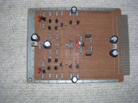
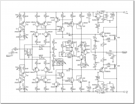
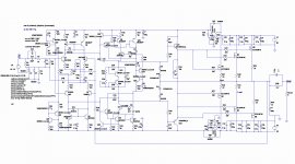
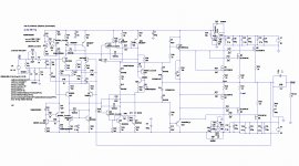
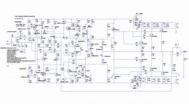
I was intrigued by the VAS topology used in Giovanni Stochino's power amplifier so I conducted a few initial experiments. These appear in the "Bryston 4B SST clone" thread as posts #132, #186, and #190. It doesn't appear to have been used much in subsequent other designs so I thought I'd try constructing a more complete amplifier on a breadboard. The schematic and a picture of the breadboard layout are shown below. Its fast, linear, and stable. Q15 and Q16 are the VAS transistors preceded by emitter followers Q13 and Q14. The two terminal current source Q17/Q20 pulls about 7mA through diode connected transistors Q18, Q19 and these in turn ensure that the VAS transistors also pass 7mA because Q15/Q18 and Q16/Q19 are current mirrors. I use the two terminal current sources shown because they have better PSRR than the more conventional two transistor types. I simply used devices and parts that were to hand to test out the topology. If I were going to use this design as the basis of a headphone or buffer amplifier I would refine it a little and use more suitable ( and expensive ) transistors. Looks to me like an idea worth exploring further.
Attachments

It's nice to see more people interested in this topology. I've made THIS post some months ago (you've even commented on it) about a similar circuit and I have finally decided to build it, I'll post the final results soon.
Your schematic looks similar to the last revision I posted on the thread above, but I found a problem with it, during stability tests, whenever I forced the amp into oscillation, the beta-enhance emitter followers (Q13 and Q14 on your pic) would misbehave and become responsible for setting the VAS current instead of the sink-source CS (Q17/Q20), the result was always at least one burnt VAS transistor, either on the NPN side or the PNP side, one charred emitter resistor and a melted spot on my breadboard.
After burning through my entire stock of BC546/556 I gave up on trying to put the VAS inside the current mirror and put the emitter follower inside of it instead, the amp could handle any oscillation after the change. The circuit I built ended up looking like an improved version of the first revision.
Another tip: I dont know what rail voltages you're using but consider cascoding the VAS transistors with TO-126 devices to reduce dissipation. During my initial tests I didn't cascode mine and was passing 7mA with ±37V rails, mere 260mW gave me a nice fingertip burn, aaand the transistors wouldn't last long working like this. Also I've found that discrete current mirrors for such high currents are NOT to be relied on.
On the plus side, after building it, I found this topology to have great stability (stable without a miller cap on a breadboard, with a square wave applied and a light capacitive load) and good symmetrical clipping behavior, please continue working on it.
When your "Push-Pull VAS" thread went quiet last year I didn't think you were pursuing the idea any further or I would have posted in that thread. We can try and get a moderator to shift these posts onto the end of yours, and continue from there if you like. In any event I'd be interested to see your latest schematic and a photo of your breadboard.
So far I haven't had any problems with torture tests. I agree with you about the stability, its rock solid. As regards cascoding the VAS transistors it makes sense, both to reduce dissipation and also because the push-pull cascodes provide better high impedance loads for each other than uncascoded VASs. I've got some background material and a schematic plus photograph of a working breadboard power amp that I'll post when we've sorted out where.
So far I haven't had any problems with torture tests. I agree with you about the stability, its rock solid. As regards cascoding the VAS transistors it makes sense, both to reduce dissipation and also because the push-pull cascodes provide better high impedance loads for each other than uncascoded VASs. I've got some background material and a schematic plus photograph of a working breadboard power amp that I'll post when we've sorted out where.
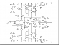
Ok next iteration. I added a lateral mosfet output stage mainly because it was the easiest to implement. So now I have either a stochino amplifier with class a input stages, an ef2 mirror vas, and lateral mosfets, or a DH220 with current mirror loaded differential pairs and a mirror vas ( DH220D? ). In any event it's still very linear, very stable, and has a clean 10kHz square wave output. More to come.
Attachments
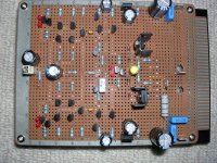
Yet another incremental improvement. Added a cascode and reduced the dissipation in Q15/Q16 by returning their collectors to the constant current bias chain rather than ground. Used BF471/BF472 for the vas because I have a stack of them with hfe clustered around 120 and they do pretty well in that position ( to126, high voltage, low capacitance ). Will use all readily available parts in the "production" version. A couple more things to try before I finalise the basic design.
Attachments

Should have said that the supply voltage is +/-42V and all of the transistors are almost exact npn/npn, pnp/pnp, npn/pnp matches. The output offset is 700uV. As an aside my transistor buying strategy has always been to buy 5 each of any complementary pair and if there's a good match order another 100 immediately before the supplier gets new batches ( hopefully ). If the match is no good then try another supplier with the same tactic, or forget it. I now have good stash of well matched complementary pairs whilst wasting hardly any money.
Interesting approach and good effort.
Have you got LT Spice asc file for this project? I have created one for your last version and got distortion about 0.1% at 20kHz. Maybe transistor models I use are different from yours or I made an error somewhere. Also used higher PS voltage, namely +/-60V but that should not affect distortion levels.
cheers,
I'm from the old style Bob Pease school "I simulate with solder" so I'm sorry I don't have an asc file. I haven't measured the distortion of the latest version yet but will do so and post results here.
Interesting approach and good effort.
Have you got LT Spice asc file for this project? I have created one for your last version and got distortion about 0.1% at 20kHz. Maybe transistor models I use are different from yours or I made an error somewhere. Also used higher PS voltage, namely +/-60V but that should not affect distortion levels.
cheers,
I sim this topology with OITPC compensation, using 90VDC and have THD: 367W/8Ohm, 20kHz -> 0.000878%.
Janusz I've just done some measurements and you're quite right. With 12.5W output at 10 kHz the second harmonic is at -70dB so I've missed something somewhere. bimo do you have a schematic of your project that you could share?
Yes, attached is asc file for 20k. Frequency can be changed. At 2k distortion is about 0.02% but at 20k it's dismal.
I transformed my Stochino with 3 lateral mosfet outputs into your version so I kept a few old transistors. I used 2sa970/sc2240 in LTP as these are much better than 2n. I have also increased gain so distortions are higher than with 20k/1k nfb but is shows how vulnerable it is to small component changes.
cheers,
PS I have added a trimpot between ltp emitters and a 100k resistor to the nfb. This allows control of DC output and does not affect distortion levels.
Attachments
Last edited:
Hi januz, thanks for your .asc file - unfortunately ltspice is not available for linux, which I use exclusively. Maybe its time to embrace the dark side. An ltspice screenshot showing your schematic would be very much appreciated, if possible. If I understand you correctly you mean that swapping the 2N5401/2N5551 for 2SA970/2SC2240 in the input ltps results in a significant thd reduction at 20kHz? What is the thd20 for your amplifier? Did you use 2SA970/2SC2240 for the current mirrors also? I've got a stash of these so I'll use them for my next prototype. I also have some 2SA1085/2SC2547 which are even better than the 2SA970/2SC2240 so I might try them also. My prototype only has one output pair with a quiescent current of 40mA ( small heatsink ) which is hardly likely to result in low distortion. I'm also a bit of a cheapskate in that I tend to make my prototypes from low cost, disposable components. At least that characterises the worst case performance ( my excuse anyway )!
The reason I used 2sa970/sc2240 in ltp is that N and P can be matched. I managed to get distortion down to about 3.5% at 20kHz.
In mirrors I used 2N2222A and 2N2907P as in the original Stochino as I converted Stochino amp into your version. For red led I used one from my LT Spice data base. Also used Sanken drivers to drive Exicons, which I have while SB/SD drivers are obsolete. 2sa1930 / 2sc5171 can also be used as well some other transistors. JPEG image is attached so you can see what is in my asc file.
cheers,
PS new asc is attached with transistors you have used in capacitance multipliers.
Attachments
Hmm interesting. My prototype measures better than your sim but the hf distortion is still too high. I notice that Stochino has 1k5 resistors in the bases of the vas current mirror transistors, presumably to isolate the vas transistor from the current setting transistor. I wonder if adding these to your sim makes any difference?
Yes, with 1k5 resistors as in the original Stochino distortion drops down to 0.011% at 20k but it is still much higher than in my simulation of my Stochino with irfp240/9240 mosfets and 2sa1407 (Q11) and 2sc3601 (Q12) in VAS - 20k distortion is 0.0006%.
I think you have unnecessarily complicated this circuit. I do not know what was your main objective in redesigning Stochino amp. Tomorrow I'll simulate your first vesion with 1k5 resistors in VAS.
cheers,
I think you have unnecessarily complicated this circuit. I do not know what was your main objective in redesigning Stochino amp. Tomorrow I'll simulate your first vesion with 1k5 resistors in VAS.
cheers,
Thanks for the feedback janusz. Of course I overcomplicated the circuit because I wanted to try everything and see what gave benefit and what did not. That's the way I tend to work - chuck the kitchen sink at it and then gradually remove stuff whilst ( hopefully ) maintaining performance. I suspected that the 1k5 resistors were important but left them out to see what happened - disaster obviously! The irfp240/9240 vertical mosfets have much higher transconductance that the ECX10N20/ECX10P20 lateral mosfets so lower distortion is to be expected - be even lower if bjt output devices were used I expect.
BTW I didn't set out to redesign the Stochino amp I wanted to test out the mirror vas in a different setting. I used a conventional input stage but Stochino uses a fast, high current classAB input stage. I think the mirror vas topology has been tried with a Sansui diamond differential input stage, which is also fast and able to deliver high current, to good effect.
OK, trying various possibilities to expand knowledge makes sense. Advantage of Stochino's amp is its speed so transient distortions are practically eliminated.
Nevertheless, it seems to me that Stochino chose to sacrifice eg thd's for speed. Thd's of his original design at 20kHz are 20 times higher than 0.0006% in my version. Anyway, I'd keep Stochino's approach to symmetrical ltp input, which is pretty standard except for clamp diodes to get speed. Instead of that 100 ohm resistor between ltp's emitters paralleled by 1nF cap, which apparently somewhat further increases speed (as well as distortion) I'd go for a trimpot and a 100k or so resistor to nfb as this allows for offset reduction at the output and this with 2N transistors can be well over 10 mV.
I'll try simulating your first VAS version with your and Stochino's input versions. Hopefully I'll have one tomorrow as today I did not have enogh time to do this.
cheers,
Last edited:
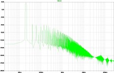
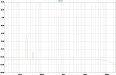
I have run simulations. Version 1 has higher distortion at 20k (0.94%) but only a few higher harmonics as can be seen in attached file.
By changing a few components (eg bias control circuit based on ksa1381/ksc3503 plus a few resistor values) distortion drops to 0.0095% at 20k but has more higher harmonics than version 1- see attached files.
So your first approach has a few merits.
cheers,
By changing a few components (eg bias control circuit based on ksa1381/ksc3503 plus a few resistor values) distortion drops to 0.0095% at 20k but has more higher harmonics than version 1- see attached files.
So your first approach has a few merits.
cheers,
Attachments
Last edited:
Ah Now I understand. Let me say that my "first approach" in post #1 was designed to drive a single pair of bjt output devices in class a at a quiescent current of approximately 15mA. I set it on the low side because I didn't have heatsinks on the BD139/40. The quiescent current is set by the ratio of R20 to R26+R27. If you had simmed this circuit exactly as posted you would have found an acceptable value of thd20. Adding an extra pair of output devices and employing a heatsink would give you a pretty good headphone amplifier. Saying that the approach has "few merits" without building or simming it is a bit sweeping.
I never suggested that the biasing scheme used in post #1 is capable of general application as you have assumed in your first schematic of post #19. This results in a gross underbiasing of the bjt/mosfet output stage so that it runs in class b with subsequent high levels of crossover distortion.
In posts #4 and #5 I kept essentially the same front end but added an emitter follower buffered mosfet output stage with an appropriate biasing scheme. I set the quiescent current to 40mA initially because I wasn't using a large heatsink. Once again the circuit, exactly as drawn, has an acceptably low thd20 bearing in mind the low quiescent current the, single pair of output devices, the lack of 1k5 resistors, and a few other minor tweaks. In fact your post #19, second schematic, is substantially the same as my post #5, except for the extra output devices. The performance is also very similar. So why did you run a sim with a known to be inadequate biasing scheme?
My "concept" here relates to the front end - all of the output stages discussed here are pretty generic. Did you ever build a Stochino amp with three pairs of Exicon mosfets?
- Home
- Amplifiers
- Solid State
- Mirror VAS