Hi,
Its been awhile, really rusty, decided to build another mini Aleph.
I checked the rail voltages about +/- 14VDC with a 12V 400VA antek.
I have CL60's on each primary.
No power shorts, nothing seems shorted to chassis or Gnd. Im using Brian's black boards, latest version. -Sig tied to ground.
When I power on I measure -14V at the speaker outputs for both channels, no load connected.
Im using star ground, Neg. Speaker terminals are going back to star ground.
The pos. Speaker terminal wired to pcb output.
The gnd and cgnd on the pcb are going to star ground.
I did install a 500ohm trimmer on R6 and preadjust to 250ohms.
DC offset should never be that high??? Looks like its just
Seeing the -14VDC power rail at the speaker output.
I will pull the pcb off and inspect again. I did not measure any shorts
At the irp240's.
Thanks for your help
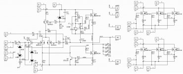
post exact schm an I'll tell what to measure
Schematic attached. R6 has a 500ohm trimmer.
I went through older threads, Q3 might be bad?
All brand new parts and I did match the Q1&Q2.
Thanks ZM
Attachments
R8 5.10 5.12
R18 9.08 9.08
Z5 8.85 8.86
R14 12.75 12.43
R27 0.34 0.35
R28 0.33 0.34
Q6 cold
Q7 warm
Voltage rails +\- 14.9V
Speaker outputs -14.4V
Inputs grounded No Load
Resistor values installed
R14 47.5K
R12 750
R17 100
R27 0.33
R28 0.33
R23 0.47
R24 0.47
R25,R26 DNI
R18 9.08 9.08
Z5 8.85 8.86
R14 12.75 12.43
R27 0.34 0.35
R28 0.33 0.34
Q6 cold
Q7 warm
Voltage rails +\- 14.9V
Speaker outputs -14.4V
Inputs grounded No Load
Resistor values installed
R14 47.5K
R12 750
R17 100
R27 0.33
R28 0.33
R23 0.47
R24 0.47
R25,R26 DNI
Last edited:
R8 5.10 5.12
R18 9.08 9.08 ---> to high that why at output -14,4V --> check circuit ,change new Q1&Q2.
Z5 8.85 8.86
R14 12.75 12.43
R27 0.34 0.35
R28 0.33 0.34
Q6 cold
Q7 warm
Voltage rails +\- 14.9V
Speaker outputs -14.4V
Inputs grounded No Load
Resistor values installed
R14 47.5K
R12 750
R17 100
R27 0.33
R28 0.33
R23 0.47
R24 0.47
R25,R26 DNI
to high that why at output -14,4V --> check circuit ,change new Q1&Q2.
not necessarily to change them
from some reason there is output offset , greater then inner LTP mosfet can rectify , that's why same one is closed - entire LTP current is going through outer mosfet
however - by memory , those pcbs are made as sort of universal , and one need to triple check how to connect things for different iterations (one or more output pairs -then placed on daughter boards)
not having them and not having any pcb file , I can't check proper position of parts
in every case - lower output mosfet is wide open , resulting in minimal voltage sag across it , and there is neg voltage at output .......
so - first complete check of parts installed and possible shorts/bad solder points and - if that is OK , desoldering input mosfets and checking them in matching jig
Last edited:
....
ZTX450 on Q6 No Good?
in this case - ZTX is certainly not the culprit
I think it's time for some pics
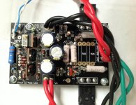
R6 500ohm trim was the culprit. I removed them and offset is now 48mV and 68mV
How long do you wait for it to get stable before measuring DC offset?
1/2hr? The offset seems to drop after few minutes, this with the top cover off.
Killawatt meter showing 100W power consumption so I think its working
How long do you wait for it to get stable before measuring DC offset?
1/2hr? The offset seems to drop after few minutes, this with the top cover off.
Killawatt meter showing 100W power consumption so I think its working
Last edited:
")
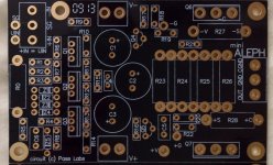
The notes I have for the posted schematic/pcb has:
R13 Bias (47.5K)
R18 DC offset (392)
R6 TBD
Would you please clarify, changing R6 vs. R18 for offset?
R6 needs to be in 10M-30Mohms. If I want to lower DC offset by 30mV,
R6 should be 20-30Mohms or lower?
So could I use 500ohm trimmer in R18?
I just want to lower the DC offset on one of the channels
If I double R13, that should bump the bias a bit?
Last edited:
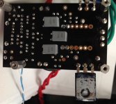
The way its mounted I cannot easily measure some of the parts.
I will have to spend some time to get all measurements.
I tried replacing Q1-Q2 matched pairs twice and still get 67mV offset after 45min
I dont understand why the offset on one channel is twice as high as the other one
I know under 100mV is ok but I want to get the offset same as other channel
2nd time I replace Q1-Q2, I also replaced Q3 and the offset is still 67mV.
I also changed R13 from 47.5k to 100k:
R27 .53v
R28 .54v
Its final bump and I will leave it. So about 1.6A bias.
Heatsink measures 43C
- Status
- This old topic is closed. If you want to reopen this topic, contact a moderator using the "Report Post" button.
- Home
- Amplifiers
- Pass Labs
- Mini Alpeh high dc offset