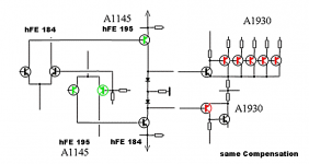
To obtain a perfectly complementary amplifier is appropriate to use components homogeneous both in the stadium in voltage at the stage at which current
to address the disparities that exist between the selected components N and P can use this configuration:
GN * GP = GRail+
GP * GN = GRail-
Grail+ = GRail-
to address the disparities that exist between the selected components N and P can use this configuration:
GN * GP = GRail+
GP * GN = GRail-
Grail+ = GRail-
Attachments
So, you are saying that to have an optimum performing amplifier, all the complementary transistors should have matched Hfe
at the quiescent conditions (idling bias). Is that what you mean?
If so, it will be a very difficult and expensive requirement, should you decide to change the bias after installing all the carefully matched parts.
at the quiescent conditions (idling bias). Is that what you mean?
If so, it will be a very difficult and expensive requirement, should you decide to change the bias after installing all the carefully matched parts.
Don't worry about bias
need just ADD a NPN (BC546) + trimmer 22K across diodes")
see new diagram for perfect gain compensation
about feedback need just a little part of partition
http://www.esafono.it/Esoter Evoque Pure Amplifier.pdf
shortly publish overview of the completed
need just ADD a NPN (BC546) + trimmer 22K across diodes
see new diagram for perfect gain compensation
about feedback need just a little part of partition
http://www.esafono.it/Esoter Evoque Pure Amplifier.pdf
shortly publish overview of the completed
Attachments
Last edited:
'Still don't follow what you are saying about device Hfe matching and why it must be done even for quite different circuit functions.
eg: The LTP and VAS transistors as shown in your first post.
This certainly conflicts with current design practice on this forum, at least.
Can you be clearer specifying what it is you are trying to tell us? I can see that you are saying the Hfe should be balanced for mirror halves,
that is a well known refinement, I believe.
Last edited:
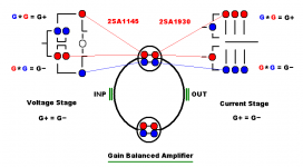
To obtain a perfectly complementary amplifier is appropriate to use components homogeneous both in the stadium in voltage at the stage at which current
to address the disparities that exist between the selected components N and P can use this configuration:
GN * GP = GRail+
GP * GN = GRail-
Grail+ = GRail-
Stee, what you show here is a quasi-complimentary output stage.
If you Google on that, you will find some additional refinements. Matching the Hfe is only limited effective, because the drivers see very different load impedances from the output devices during a signal cycle.
People like Peter Walker and I believe John Linsley Hood have studied this and came up with very good refinements.
jan
Hi,
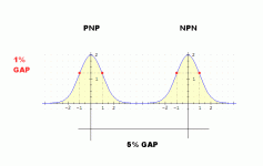
Anyone who thinks hfe can be defined to 3 significant digits
is barking up the wrong tree, same with the total hfe's
having much to do with the amplifiers gain structure.
Fabulous "pointless" features of an amplifier are just
window-dressing, bypassing thorough understanding.
rgds, sreten.
Anyone who thinks hfe can be defined to 3 significant digits
is barking up the wrong tree, same with the total hfe's
having much to do with the amplifiers gain structure.
Fabulous "pointless" features of an amplifier are just
window-dressing, bypassing thorough understanding.
rgds, sreten.
I don't believe this design outlined in the PDF addresses the issues you raised in post 1. The block diagram appears symmetrical on paper but that is about all - there is no evidence beyond concept that it has any benefit to resolving transistor complementary differences, electrically or even sonically speaking.
If you want to design worthwhile circuits, you need to understand solid-state electronics a little better to grasp how electrical and diagrammatic balance differs and what are realistic expectations for semiconductor "matching".
The bigger question is why you believe duplicating an amplifier circuit and then matching each carefully so as to rejoin them in parallel with transformers achieves anything tangible. Does it?
- Status
- This old topic is closed. If you want to reopen this topic, contact a moderator using the "Report Post" button.
- Home
- Amplifiers
- Solid State
- Method of compensation of the gains